• Advanced Photonics Nexus
  • Vol. 2, Issue 2, 026005 (2023)
Jingshu Guo1、2、†, Laiwen Yu1, Hengtai Xiang1, Yuqi Zhao1, Chaoyue Liu1, and Daoxin Dai1、2、3、*
Author Affiliations
  • 1Zhejiang University, College of Optical Science and Engineering, International Research Center for Advanced Photonics, State Key Laboratory for Modern Optical Instrumentation, Hangzhou, China
  • 2Zhejiang University, Jiaxing Research Institute, Intelligent Optics & Photonics Research Center, Jiaxing Key Laboratory of Photonic Sensing & Intelligent Imaging, Jiaxing, China
  • 3Zhejiang University, Ningbo Research Institute, Ningbo, China
  • show less
    DOI: 10.1117/1.APN.2.2.026005 Cite this Article Set citation alerts
    Jingshu Guo, Laiwen Yu, Hengtai Xiang, Yuqi Zhao, Chaoyue Liu, Daoxin Dai. Realization of advanced passive silicon photonic devices with subwavelength grating structures developed by efficient inverse design[J]. Advanced Photonics Nexus, 2023, 2(2): 026005 Copy Citation Text show less
    Proposed inverse design strategy for passive photonic devices. (a) The design framework is demonstrated by an example of a photonic device with one input port and two output ports. Here, the SWG has a period of P and a fill factor of Λ. (b) Design flow chart with manual interventions. (c) Typical manual intervention operations.
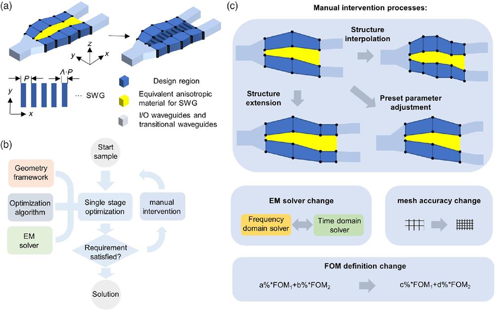
    Fig. 1. Proposed inverse design strategy for passive photonic devices. (a) The design framework is demonstrated by an example of a photonic device with one input port and two output ports. Here, the SWG has a period of P and a fill factor of Λ. (b) Design flow chart with manual interventions. (c) Typical manual intervention operations.
    Inverse design of a six-channel mode (de)multiplexer on silicon. (a) Top view (xy plane), 3D view, and cross-sectional view (yz plane) at the interface between section n−1 and section n (not to scale). (b) FOM and the simulation time cost as functions of the iteration generation for air-slot and SiO2-slot devices. Inset: the milestone structures in the optimization flow. (c) and (d) The 3D FDTD simulation performance of the designed SiO2-filled mode (de)multiplexer including the transmissions (c) and the light propagation fields for different input modes at 1550 nm (d). Modes #1 to #6 are, respectively, the TE0 to TE5 modes supported by the bus waveguides (Port #1), and modes #7 to #12 are, respectively, the TE0 mode of Ports #2 to #7. Here the silicon photonic waveguides with a 220-nm-thick silicon core and a SiO2 upper-cladding are used.
    Fig. 2. Inverse design of a six-channel mode (de)multiplexer on silicon. (a) Top view (xy plane), 3D view, and cross-sectional view (yz plane) at the interface between section n1 and section n (not to scale). (b) FOM and the simulation time cost as functions of the iteration generation for air-slot and SiO2-slot devices. Inset: the milestone structures in the optimization flow. (c) and (d) The 3D FDTD simulation performance of the designed SiO2-filled mode (de)multiplexer including the transmissions (c) and the light propagation fields for different input modes at 1550 nm (d). Modes #1 to #6 are, respectively, the TE0 to TE5 modes supported by the bus waveguides (Port #1), and modes #7 to #12 are, respectively, the TE0 mode of Ports #2 to #7. Here the silicon photonic waveguides with a 220-nm-thick silicon core and a SiO2 upper-cladding are used.
    Fabricated devices and measured results. (a) Microscope picture for the fabricated silicon PIC consisting of a pair of mode (de)multiplexers with six input ports (ITE0−ITE5) and six output ports (OTE0−OTE5). (b) SEM image of a mode (de)multiplexer. (c) Normalized transmissions of different port pairs.
    Fig. 3. Fabricated devices and measured results. (a) Microscope picture for the fabricated silicon PIC consisting of a pair of mode (de)multiplexers with six input ports (ITE0ITE5) and six output ports (OTE0OTE5). (b) SEM image of a mode (de)multiplexer. (c) Normalized transmissions of different port pairs.
    Inverse design of a 90 deg hybrid on silicon. (a) The 3D schematic diagram. LO, local oscillator. (b)–(f) The simulated performances of the final design (SiO2 slot device): the simulated light propagation fields with varied phase difference Δθ21 between Ports 2 and 1 at (b) 1550 nm, (c) the transmissions, (d) CMMRs, (e) the Els, and (f) phase errors (f). Here the transmission is given by the S parameter (i.e., Sij channel is given by 20 log10|Sij|). CMMR, common mode rejection ratio.
    Fig. 4. Inverse design of a 90 deg hybrid on silicon. (a) The 3D schematic diagram. LO, local oscillator. (b)–(f) The simulated performances of the final design (SiO2 slot device): the simulated light propagation fields with varied phase difference Δθ21 between Ports 2 and 1 at (b) 1550 nm, (c) the transmissions, (d) CMMRs, (e) the Els, and (f) phase errors (f). Here the transmission is given by the S parameter (i.e., Sij channel is given by 20log10|Sij|). CMMR, common mode rejection ratio.
    Experimental results of the fabricated 90 deg hybrid. (a) Measured transmissions. (b) Measured CMMRs. (c) Measured ELs. (d) The port-to-port optical transmission are spectra measured by the phase-test PIC. (e) Phase error extracted from the measured results of the phase-test PIC.
    Fig. 5. Experimental results of the fabricated 90 deg hybrid. (a) Measured transmissions. (b) Measured CMMRs. (c) Measured ELs. (d) The port-to-port optical transmission are spectra measured by the phase-test PIC. (e) Phase error extracted from the measured results of the phase-test PIC.
    The inverse-designed two-channel wavelength multiplexer on silicon. (a) 3D schematic diagram. (b) Simulated light propagation in the designed devices. (c) Calculated transmissions. (d) Measured transmissions. Inset: SEM image of the fabricated wavelength demultiplexer.
    Fig. 6. The inverse-designed two-channel wavelength multiplexer on silicon. (a) 3D schematic diagram. (b) Simulated light propagation in the designed devices. (c) Calculated transmissions. (d) Measured transmissions. Inset: SEM image of the fabricated wavelength demultiplexer.
    DeviceType, yearFootprint (μm2)EL (dB)CT/ER/CMMR/IM (dB)Bandwidth (nm)aSpecial indicatorsbRef.
    Sim.Exp.Sim.Exp.Sim.Exp.Sim.Exp.
    Mode (de)multiplexerDual-core adiabatic tapers, 2018∼33×471NA<1.8NACT<-141408010 Channels (5TE+5TM)37
    Tilt waveguide junctions, 20222 × 50<1<1.29CT<-17.4CT<-14.460604 Channels43
    ANN-Inverse design, 20212 × 17.5<1.1@1.55 μm)<2.4@1.55 μmCT<-10CT<-1090703 Channels44
    Inverse design, 20205.4 × 6<2 (∼1@1.55 μm)<1.5CT<-18CT<-1660604 Channels13
    Inverse design, 20216.5 × 6.5NA0∼10NACT<-14NA604 Channels14
    Inverse design, 20224.8 × 4.8<5 (<1.1@1.55 μm)<2.5CT<-12CT<-12100404 Channels12
    Inverse design7.5 × 18<1.03<∼1CT<-15.12CT<-10100906 ChannelsThis work
    90 deg hybridMMIs + phase shifter, 201721.6 × 27.9<0.45<0.5CMMR>30CMMR>303535-PE < 329
    Inverse design, 20224.8 × 4.2<2 (<0.5@1.55 μm)<2.1a)−2∼2.4 (IM)∼±2 (IM)10040PE < 70 (<6.5@1.55 μm)PE < 27 (<10@1.55 μm)12
    Inverse design4.71 × 13.03<0.96<1CMMR > 26.33CMMR>10.24040PE<4.6PE<14.9 (<5@1.55 μm)This work
    IM < 0.37IM=-2.82∼1.5
    WDMInverse design, 20152.8 × 2.8∼1.7@1.3/1.55 μm>1.8/2.4ER >∼ 13ER>11100/170100/1702 Channels, Flat-top9
    Inverse design, 20185.5 × 4.51.56/1.68/1.352.82/2.55/2.29ER > 15ER>10.7NANA3 Channels, Non-flat-top41
    Inverse design, 20191.4 × 1.80.36/0.09/0.761.87/1.49/3.47ER > 6.23ER>8.51NANA3 Channels, Non-flat-top33
    Inverse design, 20202.8 × 2.80.3/0.54NAER > 15.29NANANA2 Channels, Non-flat-top42
    4.6 × 2.8∼1.9ER = ∼ 134 Channels, Non-flat-top
    6.95 × 2.80.31∼2.12ER > 15.866 Channels, Non-flat-top
    Inverse design, 20226.2 × 5.4∼0.81.2ER > 17ER > 15>30>303 Channels, Flat-top40
    Inverse design3.07 × 12.46<1<1ER > 10ER > 1080/14088/1092 Channels, Flat-topThis work
    Table 1. Summary of the state-of-the-art mode (de)multiplexers, 90 deg hybrids, and wavelength (de)multiplexers on silicon.
    Jingshu Guo, Laiwen Yu, Hengtai Xiang, Yuqi Zhao, Chaoyue Liu, Daoxin Dai. Realization of advanced passive silicon photonic devices with subwavelength grating structures developed by efficient inverse design[J]. Advanced Photonics Nexus, 2023, 2(2): 026005
    Download Citation