Abstract
Compact passive silicon photonic devices with high performance are always desired for future large-scale photonic integration. Inverse design provides a promising approach to realize new-generation photonic devices, while it is still very challenging to realize complex photonic devices for most inverse designs reported previously due to the limits of computational resources. Here, we present the realization of several representative advanced passive silicon photonic devices with complex optimization, including a six-channel mode (de)multiplexer, a broadband 90 deg hybrid, and a flat-top wavelength demultiplexer. These devices are designed inversely by optimizing a subwavelength grating (SWG) region and the multimode excitation and the multimode interference are manipulated. Particularly, such SWG structures are more fabrication-friendly than those random nanostructures introduced in previous inverse designs. The realized photonic devices have decent performances in a broad bandwidth with a low excess loss of <1 dB, which is much lower than that of previous inverse-designed devices. The present inverse design strategy shows great effectiveness for designing advanced photonic devices with complex requirements (which is beyond the capability of previous inverse designs) by using affordable computational resources.1 Introduction
Integrated photonics1 has been known as a key technology of optoelectronics. By using on-chip light manipulations, the bulk optical and optoelectronic systems can be integrated to compact and robust photonic integrated circuits (PICs), bringing significant advantages in cost, size, and power consumption. As the integration intensity of the PICs increases, researchers have been devoted to developing advanced passive silicon photonic devices with high performance and compact footprints.2 For this problem, inverse design3–6 provides a solution. An inverse design method translates the photonic design into finding the solution for a black-box problem, in which the device structure is generated according to the given objective function by using computer-aided design methods7 [such as evolutionary algorithms (EAs) or artificial neural networks (ANNs)8]. Inverse design can break the limitation of the conventional (forward) design methods, and thus potentially results in much more compact footprints in contrast to the conventional devices.9,10
For inverse design, the set of the to-be-decided geometry parameters is usually called an “individual.” An individual and its corresponding set of the objective values consist of a “sample,” which can be used for the training of ANNs. All the possible individuals constitute the high-dimension search space. Similarly, all the objective-value set constitute the solution space whose dimension is the objective-value set dimension. As is well known, a multiobjective problem11 is widely recognized as a big challenge in the field of computing mathematics. Currently, the inverse design of photonic devices is mainly limited to low-dimension solution spaces, in which case only a few objective values are allowed to be involved. When designing a photonic device with a high-order scattering matrix, a large number of matrix elements should be optimized simultaneously, which makes the design optimization pretty difficult. For example, there are few results of demonstrating the inverse design of a 90 deg hybrid because the optimization is challenging when both amplitude and phase responses of all four output ports are considered.12 Similarly, the design complexity for mode (de)multiplexers increases significantly with the channel number, and thus currently the mode (de)multiplexers demonstrated with an inverse design still have quite limited mode channels (no more than four).12–14 Therefore, it is still very desirable to develop an improved inverse design approach available for developing advanced passive silicon photonic devices with functional complexity.
To solve a black-box problem, a technical route is utilizing optimization algorithms, such as the evolutionary algorithms (EAs),15 the search algorithms (e.g., binary search algorithm10), and the gradient-based algorithms (e.g., gradient descent optimization9 and topology optimization16). The geometry framework is usually a complete black box with a very high search space dimension (e.g., 100–10003,9,10,12–14). The most popular geometry frameworks for the fully atomic inverse design are the complete black-box structures, such as no-shape-constraint topology optimization structures6,9,14 and pixel structures,10,12,13 both of which have to introduce a high search space dimension (at a scale of ). To design application-oriented photonic integrated devices with decent performances, the multiobjective problems should be solved efficiently even when no reasonable initial individual is available. In this case, the optimization convergence usually becomes very difficult due to the high-dimensional search space and the high-dimensional solution space, and huge computational resources are needed. Moreover, the region to be designed is usually very limited (e.g., typically 9,10,12–14,17) in order not to introduce an unacceptable search space dimension (e.g., ). However, the device performance might not be sufficiently excellent for real applications due to the limited solution space. As a result, the fully atomic inverse design usually cannot perform well for complex functional devices of photonics, e.g., the obtained performance may not meet the application requirements. From the perspective of device fabrication, the device generated from the fully automatic inverse design usually has a very tiny feature size, and the structure might be highly nonuniform, which makes the fabrication requirement very crucial. As an alternative, recently ANNs have provided another technical route for inverse design.8,18 It has been reported that a well-trained forward-modeling ANN may solve a nanophotonic particle inverse-design problem much more efficiently than optimization algorithms.19 However, the training of the ANN still requires a large amount of computing resources. In Ref. 19, there are as many as 50,000 samples needed to train a forward-modeling ANN for an eight-sample-dimension problem. Therefore, the ANN inverse design mainly focuses on the specific grating design problems with low search space dimension of 8,18 and, consequently, it is highly desirable to reduce the dimension.20,21
Sign up for Advanced Photonics Nexus TOC. Get the latest issue of Advanced Photonics Nexus delivered right to you!Sign up now
As discussed in Ref. 22, the issue for the fully automatic inverse design may be solved with the prior knowledge and intuition of experienced designers, in which the computational costs can be reduced by applying intelligent constraints and supplying an exceptional initialization. Previously, we proposed a universal manipulation strategy of on-chip multimode excitations/interferences by using all-dielectric metamaterial waveguides, and mode exchangers were successfully designed with low computation cost.23 Fundamentally, various on-chip photonic devices for light manipulations with their amplitudes,24 wavelengths,25 polarizations,26 phases,17 as well as modes27 can be realized by appropriately manipulating the mode excitations and the mode interferences.
In this work, we propose a high-efficiency inverse design approach for developing advanced passive silicon photonic devices based on branch waveguides with subwavelength grating structures. Supervised by the theory of multimode excitations/interferences,23 this geometry framework enables a high degree of freedom and low search space dimension of to simultaneously. Importantly, it naturally supports a multistage optimization strategy with manual intervention. Benefiting from the experiences of traditional designs, the dimension of the search space increases minimally during the design process, which simultaneously enables fast convergence and high design flexibility. Meanwhile, some advanced optimization algorithms [like covariance matrix adaptation evolution strategy (CMA-ES)] and efficient electromagnetic (EM) simulation tools are applied to further improve the computational efficiency. Finally, three representative devices are designed and fabricated, confirming the effectiveness of the present approach for handling complex multiobjective problems. Furthermore, the designed photonic devices presented here are based on subwavelength grating structures and thus have good feature-size uniformity, which can be fabrication-friendly.
2 Results
2.1 Theory and Strategy
For an inverse design, there are two key points to improve the design efficiency. First, the search space dimension should be minimized as much as possible. Second, the search space should be well-defined so that the final optimal design is included. As a result, in this paper, we propose an inverse design method with unique features that are useful for efficiently developing advanced passive silicon photonic devices, as described below.
2.1.1 Device geometry definition
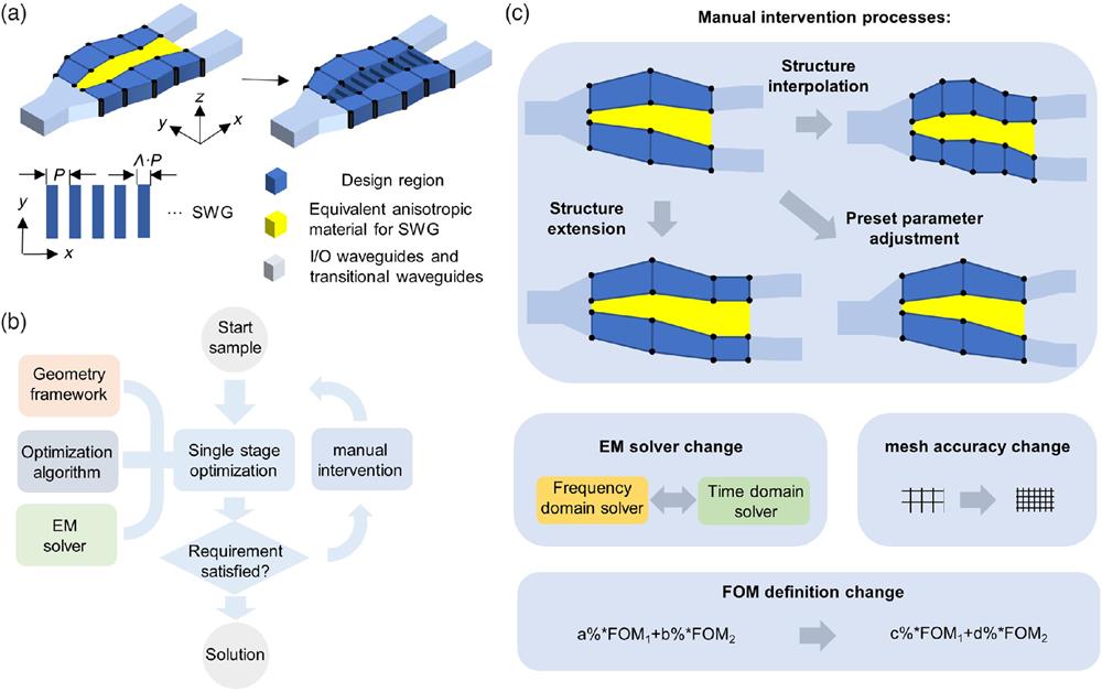
The device structure is basically defined geometrically with some waveguide branches separated by subwavelength grating (SWG) metamaterial structures, as shown by the example given in Fig. 1(a). Definitely, the devices with more ports have more branches. Here each branch [see the deep-blue part in Fig. 1(a) which consists of several segments longitudinally, and each segment is defined by its corner locations (i.e., the black pillars in Fig. 1(a)]. As shown in Fig. 1(a), an SWG structure is usually defined by the period and the fill factor , which can be preset or adjusted freely as desired. The SWG structures enable the dispersion engineering to realize broadband or wavelength-sensitive photonic devices when desired.23,28 These to-be-designed geometry parameters are included in the individual for the optimization.23

Figure 1.Proposed inverse design strategy for passive photonic devices. (a) The design framework is demonstrated by an example of a photonic device with one input port and two output ports. Here, the SWG has a period of and a fill factor of . (b) Design flow chart with manual interventions. (c) Typical manual intervention operations.
This device geometry definition is derived from our previous work,23 where a universal strategy of on-chip multimode excitation/interference was demonstrated. In this work, the optimization of the design region enables flexible mode manipulation and further realizes on-chip light manipulations. The present design strategy is potentially useful as a universal approach for developing various optical functional devices even without any special initialization. This is different from those previously reported works based on multisectional multimode interferences (MMIs) optimized with appropriate initialization.24,29 In particular, the multibranch structure proposed here as the initialization can build up a relatively smooth connection between the input/output ports and the design region. As a result, it is possible to achieve excess losses (ELs) lower than those of previous inverse design devices with random nanostructures.
Apparently, the search space dimension is decided by the number of the lengthwise sections in the design region. Any design region with sections can be redefined with sections when needed. Such flexibility in the design makes it convenient to gradually adjust the search space dimension. For example, a low search space dimension with, e.g., only can be adopted at the first stage of the optimization, so that one can achieve a suboptimal solution with a low computational cost. The suboptimal solution can be further used to initialize the second stage of optimization for which the search space dimension is improved to be with . In this way, the present approach has much higher capability for the optimization of complex photonic devices even with limited computational resources than those of previous inverse design approaches.
2.1.2 Iteration strategy with manual interventions
Figure 1(b) shows the design flow chart of the present inverse design method, which is based on a multistage optimization iteration strategy with manual interventions. One stage of optimization is terminated when the figure of merit (FOM) comes to a standstill. The corresponding solution is then used to initialize the next stage of optimization, and manual interventions may be introduced in the initialization, the EM solver setting, or other parameter setting. Figure 1(c) gives several kinds of typical manual intervention processes, which include the following cases. (1) The search space dimension can gradually be increased as the optimization stage iterates. For example, as shown in Fig. 1(c), a stage solution with two sections and 12 definition corners can be used to derive new generation with four sections and 20 definition corners. (2) When possible, one should first use the most efficient EM solver in the early stages of optimization and then use a high-precision EM solver (which is usually time-consuming) for the final stages of optimization. (3) For a multiobjective problem with a high-solution space dimension, the definition of the FOM may also be modified manually as the optimization stage iterates to balance the optimizations of different objective values [Fig. 1(c)]. (4) When no gratifying solution is obtained after several stages of optimizations, the global settings of the computation need to be modified. For example, the design region can be extended by the structure extension process. The preset parameters (like the input/output waveguide locations) can also be changed, as shown in Fig. 1(c).
Assisted with some manual interventions, the present inverse design with the multi-stage optimization strategy has a high potential to realize high-performance functional photonic devices, since the search-space dimension for the final-stage optimization could be sufficiently high. Meanwhile, the optimization can be efficient because the geometry definition strategy is used to reduce the search-space dimension significantly.
2.1.3 Optimization algorithm
We use the covariance matrix adaptation evolution strategy (CMA-ES),30 which is known as an advanced optimization algorithm solving difficult black-box problems with large budgets. CMA-ES and its variants have been found to outperform other optimization algorithms when the search space dimension is high (e.g., ).15,31 Currently, there have been few works using CMA-ES for the inverse designs of photonic integrated devices.32 In this work, this advanced optimization algorithm is introduced to be helpful for efficient inverse designs. More details about this algorithm are given in the Appendix, Sec. 4.1.
2.1.4 EM simulation tool
To evaluate the FOM, the EM simulation should be carried out for each individual. The typical EM simulation tools include finite-difference time-domain (FDTD),10 finite-difference frequency domain (FDFD),7 finite-element method (FEM),33 and eigenmode expansion (EME).34 The EM-solving simulations usually occupy most of the computational resource in inverse designs. Apparently, the simulation time usually increases with the device footprint.
EME is also a frequency-domain algorithm whose computation speed and precision depend on the number of the eigenmodes involved and the number of the sections along the light propagation direction (rather than the device footprint).35 With EME, the total scattering matrix for all the ports of the device can be achieved in one run. In this case, only one run is needed even for a six-channel mode demultiplexer (DEMUX) (with six output ports). In contrast, one has to run the FDTD simulation six times for the six mode channels one by one. Furthermore, an EME simulation may be much faster than a 3D FDTD simulation when the device has a large footprint (e.g., the ). However, the EME method does not work well when there are sharp bends or nonwaveguide structures. Fortunately, the initialized structure is defined very well and thus intrinsically satisfies the requirement of EME.
Therefore, in this paper, the EME method is introduced as an important tool for the simulation. In the early stages of optimizations, EME is used to obtain a preliminary optimization solution, which is then used as a good initialization for the following optimization stages with a 3D FDTD simulation. For example, when designing a six-channel mode DEMUX, the EME simulation takes 80.6 h only to improve the FOM from 10.94 to 0.42. The preliminary solution obtained by the EME simulation is already very close to the final optimization result. The introduction of efficient EME helps greatly to improve the efficiency of our inverse design method for developing high-performance optical functional devices.
In short, the present inverse design method combines the search-space-dimension-control strategy, the advanced optimization algorithm, and the flexible EM simulation strategy, so that it enables to solve efficiently multiobjective optimization problems. In the following sections, several advanced passive silicon photonic devices are presented by utilizing this inverse design method. In contrast, the design of these devices is very challenging due to the complexity when using previous inverse design methods.
2.2 Realization of a Six-channel Mode (de)multiplexer
A mode (de)multiplexer is the fundamental device in mode-division-multiplexing systems. Typically, high-performance mode (de)multiplexers are often realized by utilizing multi-stage asymmetric directional couplers.36,37 Recently, ultracompact mode (de)multiplexers have been demonstrated by using the inverse design methods.12–14 However, these inverse-designed modes (de)multiplexers have no more than four channels. The reason is that the inverse design becomes much more difficult due to the increased complexity when it is desired to be with more channels (more ports).
Here, we propose and demonstrate a six-channel mode (de)multiplexer for the first time by utilizing the inverse design method. As shown in Fig. 2(a), the initial geometry framework is based on an ordinary branch configuration without special considerations. In the optimization region, there are six polygon waveguides defined in the following way. Along the lengthwise direction, there are sections defined with the lengths . At the cross-sectional interface between the ()’th and the ’th sections, the parameters define the lateral corner location in the direction [see Fig. 2(a)]. The metamaterial SWG structure has a period and a fill factor . Specifically, here we choose and . For the input/output (I/O) waveguides, and respectively denote the waveguide widths, and respectively denote the positions of Port #1 and Port #7 in the axis, and is the separation between the adjacent output waveguides. The parameter () denotes the length of the waveguide taper connecting the optimization region and the input (output) waveguide. The parameter set to be optimized can combine flexibly any related parameters. For example, one might have or .
Figure 2.Inverse design of a six-channel mode (de)multiplexer on silicon. (a) Top view ( plane), 3D view, and cross-sectional view ( plane) at the interface between section and section (not to scale). (b) FOM and the simulation time cost as functions of the iteration generation for air-slot and -slot devices. Inset: the milestone structures in the optimization flow. (c) and (d) The 3D FDTD simulation performance of the designed -filled mode (de)multiplexer including the transmissions (c) and the light propagation fields for different input modes at 1550 nm (d). Modes #1 to #6 are, respectively, the to modes supported by the bus waveguides (Port #1), and modes #7 to #12 are, respectively, the mode of Ports #2 to #7. Here the silicon photonic waveguides with a 220-nm-thick silicon core and a upper-cladding are used.
For the scattering matrix of a photonic device, the element denotes the coupling coefficient from mode to mode . For the six-channel mode (de)multiplexer considered here, the bus waveguide at Port #1 supports six modes (i.e., the modes denoted as modes #1–#6). The output waveguides at Ports #2–#7 support the corresponding modes (denoted as modes #7–#12). Ideally, a six-channel mode (de)multiplexer should have the transmissions of , where , , and . The FOM for optimization is defined by . Even though the optimization was run with a single operation wavelength of , fortunately, the optimized photonic device is very possible to work very well with a broad bandwidth, which is attributed to the dispersion-insensitive multimode excitation/interference processes in the SWG waveguides, as demonstrated previously.23
Figure 2(b) shows the FOM and the total computation time cost as the iteration generation updates. The computation time was evaluated on an ordinary personal computer (PC; details in Appendix, Sec. 4.2). The milestone structures generated during the optimization are also depicted in Fig. 2(b). One can see that an ordinary branch waveguide structure is used as the initial individual. In terms of the fabrication process, the filling in the SWG slots usually depends on the deposition technology. In the design, we consider the cases with air slots or slots. The air-slot device was designed first with a regular linear initial structure [Fig. 2(b)]. The EME method was used at the early stages, and the FOM reaches 0.42 dB after 384 generations of iteration (80.6 h). The FDTD simulation with two types of mesh precision (see the details in Table S1 in the Supplementary Material) was then used in the following stages of optimization. Finally, the FOM is about 0.69 dB, obtained with 104 generations (41.5 h). This corresponding design was then used as the initialization for further optimizing the air-slot and -filled devices with high-precision FDTD simulation. As shown in Fig. 2(b), the optimization of the air-slot device finishes at the 507th generation with an FOM of 0.55 dB, costing 247.1 h in total. And the optimization of the -filled device finishes at the 590th generation with an FOM of 0.62 dB, costing 419.2 h in total (including the 122.1 h for the optimization of the air-slot device initially). For such multistage designs, manual intervention processes were carried out. For example, the section number changes from 6 to 24. More details are given in Sec. S1 in the Supplementary Material. The two types of devices have similar theoretical performances, providing excellent options for the labs/fabs with different fabrication technologies. In the following section, we focus on -filled devices regarding the fabrication technologies available.
According to the high-precision 3D FDTD simulations with very fine meshes (26 mesh points per effective-wavelength scale), the designed -filled device (with detail geometric parameters in Table S2 in the Supplementary Material) has a footprint as compact as , low ELs from 0.53 to 1.03 dB, and low cross talks (CTs) in the wavelength range from 1500 to 1600 nm for all mode channels, as shown in Fig. 2(c). In Fig. 2(d), the simulated light propagation at 1550 nm is given, showing impressive mode (de)multiplexing behaviors. The devices were fabricated by the regular processes from Applied Nanotools Inc.38 (details in Appendix, Sec. 4.3). Figure 3 shows the experimental results. Here the measured PIC consists of a pair of mode (de)multiplexers and fiber-to-chip grating couplers [see Fig. 3(a)]. Figure 3(b) shows the scanning electron microscope (SEM) image of the fabricated device, and the normalized transmissions of the PIC are shown in Fig. 3(c). It can be seen that all channels for the fabricated mode (de)multiplexers have a low EL of and low CT of in the wavelength range from 1520 to 1610 nm experimentally. The slight ripples in the transmission spectrums may be attributed to the nonzero reflection of the mode (de)multiplexers.
Figure 3.Fabricated devices and measured results. (a) Microscope picture for the fabricated silicon PIC consisting of a pair of mode (de)multiplexers with six input ports () and six output ports (). (b) SEM image of a mode (de)multiplexer. (c) Normalized transmissions of different port pairs.
2.3 Realization of a 90 deg Hybrid
A 90 deg hybrid is the key device in optical coherent communication systems. Basically speaking, a 90 deg hybrid has two input ports [i.e., Port #1 for the signal and Port #2 for the local oscillator (LO)] and four output ports (#3, #4, #5, and #6), as shown in Fig. 4(a). Generally speaking, the optimal design of a 90 deg hybrid is pretty challenging because not only the amplitude responses but also the phase responses at the four ports should be considered.
Figure 4.Inverse design of a 90 deg hybrid on silicon. (a) The 3D schematic diagram. LO, local oscillator. (b)–(f) The simulated performances of the final design ( slot device): the simulated light propagation fields with varied phase difference between Ports 2 and 1 at (b) 1550 nm, (c) the transmissions, (d) CMMRs, (e) the Els, and (f) phase errors (f). Here the transmission is given by the parameter (i.e., channel is given by ). CMMR, common mode rejection ratio.
For a 90 deg hybrid, the scattering matrix of the electric field amplitude should satisfy eight requirements of (; ), while the phase differences between the output ports should satisfy the condition of , where . In this problem, there are 11 target values, including eight amplitude requirements and three phase requirements. One should notice that the correlation of these target values is weak in the optimal design of a 90 deg hybrid. Specifically, the amplitude-target-value-set for Port #1, the amplitude-target-value-set for Port #2 and the phase-target-value-set have almost no correlation among them. In this case, the optimization is often likely to be trapped locally, and it is hard to reach the globally optimal design. Nevertheless, the present high-efficiency inverse design works well and gives a high-performance 90 deg hybrid successfully. As shown by the details in Sec. S2 in the Supplementary Material, the FOM definition can be adjusted manually in the multistage optimization process to ensure global optimization for all the target values.
Finally, the 90 deg hybrid is designed with a footprint of (with detail geometric parameters in Table S3 in the Supplementary Material), and one has . As a result, Ports #3 and #4 are the in-phase () channels, while Ports #5 and #6 are the quadrature () channels. Figure 4(b) shows the simulated light propagation when the modes with different phase differences are, respectively, injected into the two input ports. One can clearly see that the interference cancellation happens at one of the four output ports according to the phase difference. It proves that the present design method is effective even when both the amplitude and phase responses are required to be considered. Figures 4(c) and 4(d) show the simulated amplitude and phase responses in the wavelength range from 1530 to 1570 nm. It can be seen that the transmission losses are 6.6 to 7.4 dB and the ELs29 of the signal- and LO-ports are , while all the phase errors are within , and the common mode rejection ratio (CMMR29) are for all channels.
Figure 5 shows the measurement results of the fabricated 90 deg hybrid. In our experiments, the transmissions were measured with the testing PIC [Fig. 5(a)], while the CMMRs and the ELs are extracted from the measured transmissions. As shown in Fig. 5(b), the measured transmissions are in the wavelength range from 1530 to 1570 nm. The CMMRs of both channels are below , and the measured ELs are below 1 dB, as shown in Fig. 5(c). The phase responses were measured by the testing PIC consisting of a power splitter, a pair of asymmetric interference arms, a 90 deg hybrid, as well as grating couplers (see Fig. S1 in Sec. S2 in the Supplementary Material), which has been widely used before.29 The measured transmissions at the four outports are presented in Fig. 5(d), and the extracted phase errors are given in Fig. 5(c), which shows that the phase error in the wavelength range from 1530 to 1570 nm is within the range from to 10.63 deg.
Figure 5.Experimental results of the fabricated 90 deg hybrid. (a) Measured transmissions. (b) Measured CMMRs. (c) Measured ELs. (d) The port-to-port optical transmission are spectra measured by the phase-test PIC. (e) Phase error extracted from the measured results of the phase-test PIC.
2.4 Realization of a Two-channel Flat-top Wavelength-Division (De)multiplexer
A wavelength (de)multiplexer39 is a key element to separate/combine different wavelength channels in wavelength division multiplexing (WDM) systems. Here, a two-channel wavelength (de)multiplexer is designed optimally with the present inverse design method. Currently, there have been several inverse designs for the wavelength (de)multiplexers with two channels,9 three channels,33,40,41 and six channels,42 and most of them are narrowband. As it is well known, a flat-top response is often desired in practice because it becomes tolerant of some random wavelength variation. For the design of a wavelength (de)multiplexer with a flat-top spectral responses, the inverse design is usually challenging because it is required to include multiple objective values. In this example, the two wavelength-channels from 1290 to 1330 nm and 1470 to 1570 nm are considered.
Basically, the two-channel wavelength (de)multiplexer has an input Port (#1) and two output Ports (#2 and #3), as shown in Fig. 6(a). The 1550 nm channel and the 1310 nm channel are launched from Port #1 and are then separated to Port #2 and Port #3, respectively. Here we choose several key wavelengths with a spacing of 20 nm for each channel, and the condition for the optimization is given by , and , . The optimization costs 302.5 h (see more details in Sec. S3 in the Supplementary Material). Finally, the designed device has a compact footprint of (with detail geometric parameters in Table S4 in the Supplementary Material). Figure 6(b) shows the simulated light propagation for the two central wavelengths by using the 3D FDTD method. As shown in Fig. 6(c), the designed wavelength (de)multiplexer has ELs of and ERs of in the wavelength ranges from 1250 to 1330 nm and 1470 to 1610 nm. The ELs at 1310 and 1550 nm are, respectively, 0.67 and 0.36 dB, while the corresponding ERs are, respectively, 15.02 and 30.33 dB. The fabricated wavelength (de)multiplexer [see the inset in Fig. 6(d)] was then measured with the help of the PICs with different grating couplers working at the corresponding wavelength bands of 1310 and 1550 nm. From the measured transmissions shown in Fig. 6(d), it can be seen that the EL is and the ER is in the wavelength ranges from 1256 to 1344 nm and 1482 to 1591 nm.
Figure 6.The inverse-designed two-channel wavelength multiplexer on silicon. (a) 3D schematic diagram. (b) Simulated light propagation in the designed devices. (c) Calculated transmissions. (d) Measured transmissions. Inset: SEM image of the fabricated wavelength demultiplexer.
2.5 Comparisons and Perspective
Table 1 gives a summary of various related silicon photonic devices reported. The state-of-the-art devices developed by conventional (forward) design methods and inverse design methods are listed. Here, the devices are evaluated by their performance within the whole bandwidth except those non-flat-top wavelength (de)multiplexers and those labeled with “@ .” Here, “@ ” is for the performance at the central wavelength . The conventional (forward) design methods usually have advantages in device performance and the design scalability. For these devices, however, the difficulty of footprint shrinking is the key issue. In contrast, inverse designs have natural advantages in footprint compactness, while the bottleneck is the design efficiency for complex functional devices with a large number of to-be-optimized objective values, such as multichannel devices or flat-top wavelength-selective devices. As shown in Table 1, the present mode (de)multiplexer exhibits high theoretical performances of low ELs, low CT, and large bandwidths comparable to or even better than those of conventional mode (de)multiplexers.37,43 The measured CT for the fabricated mode (de)multiplexers is slightly inferior to conventional mode (de)multiplexers, and the footprints depend on the channel numbers. More recently, a four-channel mode (de)multiplexers using tilt waveguide junctions was reported with footprint of ,43 which represent the state-of-the-art level of the conventional methods. Definitely, the device footprint will increase greatly if the channel number increases from 4 to 6. Furthermore, the performance degradation may occur as usual. To the best of our knowledge, we present the first six-channel mode (de)multiplexers developed with inverse design, owing to the high efficiency of our inverse design strategy. Moreover, our devices have advantages in the performances of the EL and the bandwidth when compared to the other inverse design counterparts.
| Device | Type, year | Footprint () | EL (dB) | CT/ER/CMMR/IM (dB) | Bandwidth (nm)a | Special indicatorsb | Ref. |
| Sim. | Exp. | Sim. | Exp. | Sim. | Exp. | Sim. | Exp. |
| Mode (de)multiplexer | Dual-core adiabatic tapers, 2018 | ∼33×471 | NA | <1.8 | NA | CT<-14 | 140 | 80 | 10 Channels (5TE+5TM) | 37 |
| Tilt waveguide junctions, 2022 | 2 × 50 | <1 | <1.29 | CT<-17.4 | CT<-14.4 | 60 | 60 | 4 Channels | 43 |
| ANN-Inverse design, 2021 | 2 × 17.5 | <1.1@1.55 μm) | <2.4@1.55 μm | CT<-10 | CT<-10 | 90 | 70 | 3 Channels | 44 |
| Inverse design, 2020 | 5.4 × 6 | <2 (∼1@1.55 μm) | <1.5 | CT<-18 | CT<-16 | 60 | 60 | 4 Channels | 13 |
| Inverse design, 2021 | 6.5 × 6.5 | NA | 0∼10 | NA | CT<-14 | NA | 60 | 4 Channels | 14 |
| Inverse design, 2022 | 4.8 × 4.8 | <5 (<1.1@1.55 μm) | <2.5 | CT<-12 | CT<-12 | 100 | 40 | 4 Channels | 12 |
| Inverse design | 7.5 × 18 | <1.03 | <∼1 | CT<-15.12 | CT<-10 | 100 | 90 | 6 Channels | This work |
| 90 deg hybrid | MMIs + phase shifter, 2017 | 21.6 × 27.9 | <0.45 | <0.5 | CMMR>30 | CMMR>30 | 35 | 35 | - | PE < 3 | 29 |
| Inverse design, 2022 | 4.8 × 4.2 | <2 (<0.5@1.55 μm) | <2.1a) | −2∼2.4 (IM) | ∼±2 (IM) | 100 | 40 | PE < 70 (<6.5@1.55 μm) | PE < 27 (<10@1.55 μm) | 12 |
| Inverse design | 4.71 × 13.03 | <0.96 | <1 | CMMR > 26.33 | CMMR>10.2 | 40 | 40 | PE<4.6 | PE<14.9 (<5@1.55 μm) | This work |
| IM < 0.37 | IM=-2.82∼1.5 |
| WDM | Inverse design, 2015 | 2.8 × 2.8 | ∼1.7@1.3/1.55 μm | >1.8/2.4 | ER >∼ 13 | ER>11 | 100/170 | 100/170 | 2 Channels, Flat-top | 9 |
| Inverse design, 2018 | 5.5 × 4.5 | 1.56/1.68/1.35 | 2.82/2.55/2.29 | ER > 15 | ER>10.7 | NA | NA | 3 Channels, Non-flat-top | 41 |
| Inverse design, 2019 | 1.4 × 1.8 | 0.36/0.09/0.76 | 1.87/1.49/3.47 | ER > 6.23 | ER>8.51 | NA | NA | 3 Channels, Non-flat-top | 33 |
| Inverse design, 2020 | 2.8 × 2.8 | 0.3/0.54 | NA | ER > 15.29 | NA | NA | NA | 2 Channels, Non-flat-top | 42 |
| 4.6 × 2.8 | ∼1.9 | ER = ∼ 13 | 4 Channels, Non-flat-top |
| 6.95 × 2.8 | 0.31∼2.12 | ER > 15.86 | 6 Channels, Non-flat-top |
| Inverse design, 2022 | 6.2 × 5.4 | ∼0.8 | 1.2 | ER > 17 | ER > 15 | >30 | >30 | 3 Channels, Flat-top | 40 |
| Inverse design | 3.07 × 12.46 | <1 | <1 | ER > 10 | ER > 10 | 80/140 | 88/109 | 2 Channels, Flat-top | This work |
Table 1. Summary of the state-of-the-art mode (de)multiplexers, 90 deg hybrids, and wavelength (de)multiplexers on silicon.
For conventional 90 deg hybrids, the state of the art is with an EL below 0.5 dB, a CMMR over 30 dB, and phase errors below 3 deg in the C-band (1530 to 1565 nm) while the footprint is .29 In contrast, the present 90 deg hybrid has a footprint shrunk by ∼tenfold and similar performances, including low ELs, high CMMRs, low phase errors, and large bandwidth. Our present 90 deg hybrid has shown much better performance on the EL, the imbalance, the phase error, and the bandwidth than those of inverse-designed 90 deg-hybrid with 2D code structures.12 The broadband characteristic of our 90 deg hybrid also reflects the high-efficiency capability of our approach for the optimization with a large number of objective values (e.g., with multiple wavelengths involved).
Nowadays, there have been many wavelength (de)multiplexers designed conventionally,39 in which high performance and footprint compactness usually conflict. As shown in Table 1, the two-channel flat-top wavelength (de)multiplexers designed with conventional methods are usually based on Mach–Zehnder interferometers,45 waveguide Bragg gratings,46 or wavelength-selective waveguide couplers,47 and they have lengths in scale of . In contrast, the inverse-designed wavelength (de)multiplexer in this work has an ultracompact footprint of . In recent years, there have been several inverse-designed wavelength (de)multiplexers.9,33,40–42 However, they most are nonflat-top.33,41,42 The inverse-designed wavelength (de)multiplexer in Ref. 9 is indeed flat-top while the EL is higher than for the central wavelengths of . In contrast, our device has flat-top responses as well as a low EL of . More recently, a three-channel flat-top wavelength (de)multiplexer was reported with a bandwidth of for an EL of and an ER of .40 In contrast, our wavelength (de)multiplexer enables flat-top responses with an ultrabroad bandwidth from 80 to 110 nm. Furthermore, the present devices can be scaled easily for more channels by structure cascading when needed.
In summary, for practical applications (e.g., optical interconnects1,2), the devices are often required to have decent performance with low losses, high extinction ratios, multiple channels, broad bandwidths, etc. As shown in Table 1, the previously reported inverse design devices usually cannot satisfy the requirement with ELs of in a broad bandwidth, which fortunately can be achieved in this work. Our designs need computation time of (see Supplementary Material) when using a single PC. This computation resource requirement is affordable even for the six-channel mode (de)multiplexer and 90 deg hybrid, which are beyond the capability of previous inverse designs with regular computational resources. As shown in Table 1, the experimental results for the CT/ER/CMMR/IM are usually inferior to the simulation ones, mainly due to fabrication errors. In our case, all the geometry parameters including and the SWG feature size are chosen to be sufficiently large (e.g., ) according to the fabrication technology. Unfortunately, there exist some acute-angle structures at some corners, which leads to some performance degradation for the fabricated devices. In the future work, the device performance (e.g., the CT) could be possibly improved by introducing smoothened subwavelength structures. The optimization efficiency should be improved further for realizing the devices with very high complexity, such as the mode/wavelength (de)multiplexers with many channels.
3 Conclusion
We have proposed a high-efficiency inverse design method for developing advanced passive silicon photonic devices with high performance and compact footprints. Multistage optimizations with manual intervention processes are carried out based on segmented geometry-definition assisted by SWG structures. Thanks to the manual intervention processes, the search space dimension increases gradually under control to realize fast convergence and high design degrees of freedom simultaneously. Meanwhile, the flexible setting of EM simulation tools and the efficient optimization algorithm CMA-ES further enable a high design efficiency for our method. Using this method, three types of advanced passive silicon photonic devices have been demonstrated, including a six-channel mode (de)multiplexer, a 90 deg hybrid, and a two-channel flat-top wavelength (de)multiplexer. In contrast to the previous inverse design methods, our method has the advantage of handling multiobjective problems and shows great potential to be applied widely for various advanced passive photonic devices. For instance, it enables the realization of the first six-channel mode (de)multiplexer designed by inverse design method, to the best of our knowledge. The first broadband 90 deg hybrid has also been realized with our inverse design, which is very challenging because there are 55 objective values involved. Furthermore, the present devices usually have low loss of , enabling the possibility of device cascading when needed. Our designs need affordable computational resources (total computation time of when using a single PC). The demonstrated devices show decent theoretical and experimental performances comparable to their state-of-the-art counterparts designed conventionally. Meanwhile, their footprints are reduced greatly by twofold to tenfold. The present work can be extended easily to III–V and lithium niobate systems. As a summary, this inverse design method is very helpful for the development of advanced passive photonic devices with high performance, design universality, and footprint compactness, which may be useful for realizing next-generation high-intensity PICs. In the future, further efforts in design strategy and computation algorithms should be made to achieve performance improvements and footprint compressions.
4 Appendix: Methods
4.1 Covariance Matrix Adaptation Evolution Strategy (CMA-ES)
CMA-ES is based on a multi-individual search in which the search individuals of each generation are sampled from multivariate normal distributions. The individuals with good FOMs are used for guiding the evolution of the normal distribution parameters. The introduction of normal distribution follows the maximum entropy principle, making this algorithm powerful. The algorithm flow is described as follows. The individuals of each generation are obtained by sampling of the normal distribution , where is the mean value of the search distribution at generation , is the step-size, and , is the covariance matrix of the normal distribution at generation . The FOM of each individual is evaluated by EM solving and then ranked. After that, part of the individuals with good FOMs (usually the better 50%) are used for updating the parameters by covariance matrix adaptation algorithm for next-generation computation (details in Ref. 30). As the generation increases, the population (including the mean value and the sampled individuals) will approach to the promising area covering good solutions. CMA-ES has been known as one of the most efficient evolutionary approaches, which is effective for the nonseparable, illconditioned black-box problems with high dimensionality. In this work, the start sample is assigned to , the initial step size is set from 2 to 7 nm, depending on the specific problems, and is an identity matrix.
4.2 Electromagnetic Field Numerical Simulation Details
The 3D FDTD simulations and EME simulations were performed by using Lumerical FDTD Solutions and Mode Solutions. In this work, the simulation time was tested on a personal computer (CPU: Inter Core i7-11700 @2.5 GHz, RAM: 64 G). The EME solver was carried with configuration of one process and 16 threads. The SWG metamaterial is equivalent to homogeneous anisotropic metamaterials.23 The FDTD solver was carried with configuration of four processes and one thread. The final performance confirmations of the devices were performed with dense meshes (i.e., mesh accuracy index of 6 or 8, corresponding to 26 or 34 mesh points per effective-wavelength scale).
4.3 Device Fabrication
All the devices were fabricated on a silicon-on-insulator (SOI) wafer with a 220 nm-thick top-silicon layer and a -thick buried dioxide layer. The silicon photonic waveguides were patterned by the processes of electron-beam lithography and inductively coupled plasma dry-etching. Then the -thick silicon dioxide cladding was deposited by using chemical vapor deposition.
Jingshu Guo is a research fellow at the College of Optical Science and Engineering, Zhejiang University. He received his BE and PhD degrees from Huazhong University of Science and Technology in 2012 and 2017, respectively. He has published over 15 papers in peer-reviewed journals. His current research interests include silicon photonics for photodetection and light manipulation.
Laiwen Yu is currently pursuing his PhD at the College of Optical Science and Engineering, Zhejiang University. He received his BE degree from Xidian University in 2019. His research interest focuses on silicon/2D material photodetectors and advanced passive photonic devices.
Hengtai Xiang is currently pursuing his PhD at the College of Optical Science and Engineering, Zhejiang University. He received his BE degree from Huazhong University of Science and Technology in 2021. His research interest focuses on silicon integrated low-dimensional material photodetectors.
Yuqi Zhao is currently a BE degree student at the College of Optical Science and Engineering, Zhejiang University. His academic pursuits and research interests lie in the design and development of advanced silicon-based photonic devices and their applications in the fields of optical communications and optical interconnects.
Chaoyue Liu received his BE and PhD degrees from Harbin Institute of Technology in 2017 and Zhejiang University in 2022, respectively. He currently works as R&D engineer at Changguang Chenxin Microelectronics Co., Ltd. His research interests include silicon integrated photodetectors and optical architecture design.
Daoxin Dai received his BEng degree from the Department of Optical Engineering, Zhejiang University (ZJU), Hangzhou, China, and his PhD from the Royal Institute of Technology, Stockholm, Sweden, in 2000 and 2005, respectively. Currently, he is the QIUSHI Distinguished Professor at ZJU and mainly works on silicon photonics. He has published >260 refereed international journal papers. He is one of the most cited Chinese researchers in 2015–2021 (Elsevier). He has given >100 plenary/tutorial/keynote/invited talks for prestigious international conferences (e.g., OFC) and also serves as the general/TPC (co) chair for many conferences, including OECC 2023 and ACP 2022. He is a Fellow of the Optica Society (formerly OSA).
References
[1] N. Margalit et al. Perspective on the future of silicon photonics and electronics. Appl. Phys. Lett., 118, 220501(2021).
[2] W. Bogaerts, L. Chrostowski. Silicon photonics circuit design: methods, tools and challenges. Laser Photonics Rev., 12, 1700237(2018).
[3] S. Molesky et al. Inverse design in nanophotonics. Nat. Photonics, 12, 659-670(2018).
[4] Z. A. Kudyshev, V. M. Shalaev, A. Boltasseva. Machine learning for integrated quantum photonics. ACS Photonics, 8, 34-46(2021).
[5] G. Genty et al. Machine learning and applications in ultrafast photonics. Nat. Photonics, 15, 91-101(2021).
[6] A. Y. Piggott et al. Inverse-designed photonics for semiconductor foundries. ACS Photonics, 7, 569-575(2020).
[7] M. M. R. Elsawy et al. Numerical optimization methods for metasurfaces. Laser Photonics Rev., 14, 1900445(2020).
[8] P. R. Wiecha et al. Deep learning in nano-photonics: inverse design and beyond. Photonics Rev., 9, B182-B200(2021).
[9] A. Y. Piggott et al. Inverse design and demonstration of a compact and broadband on-chip wavelength demultiplexer. Nat. Photonics, 9, 374-378(2015).
[10] B. Shen et al. An integrated-nanophotonics polarization beamsplitter with 2.4×2.4 μm2 footprint. Nat. Photonics, 9, 378-382(2015).
[11] B. Li et al. Many-objective evolutionary algorithms: a survey. ACM Comput. Surv., 48, 1-35(2015).
[12] H. Zhou et al. Dielectric metasurfaces enabled ultradensely integrated multidimensional optical system. Laser Photonics Rev., 16, 2100521(2022).
[13] H. Xie et al. Highly compact and efficient four-mode multiplexer based on pixelated waveguides. IEEE Photonics Technol. Lett., 32, 166-169(2020).
[14] K. Y. Yang et al. Inverse-designed multi-dimensional silicon photonic transmitters, 1-19(2021).
[15] N. Hansen et al. Comparing results of 31 algorithms from the black-box optimization benchmarking BBOB-2009. Proc. 12th Annu. Conf. Companion on Genetic and Evol. Comput., 1689-1696(2010).
[16] M. P. Bendsoe, O. Sigmund. Topology Optimization: Theory, Methods, and Applications(2003).
[17] R. Halir et al. High-performance 90° hybrid based on a silicon-on-insulator multimode interference coupler. Opt. Lett., 36, 178-180(2011).
[18] J. Jiang, M. Chen, J. A. Fan. Deep neural networks for the evaluation and design of photonic devices. Nat. Rev. Mater., 6, 679-700(2021).
[19] J. Peurifoy et al. Nanophotonic particle simulation and inverse design using artificial neural networks. Sci. Adv., 4, eaar4206(2018).
[20] D. Melati et al. Mapping the global design space of nanophotonic components using machine learning pattern recognition. Nat. Commun., 10, 4775(2019).
[21] Y. Kiarashinejad, S. Abdollahramezani, A. Adibi. Deep learning approach based on dimensionality reduction for designing electromagnetic nanostructures. NPJ Comput. Mater., 6, 12(2020).
[22] S. D. Campbell et al. Review of numerical optimization techniques for meta-device design. Opt. Mater. Express, 9, 1842-1863(2019).
[23] J. Guo et al. Ultra-compact and ultra-broadband guided-mode exchangers on silicon. Laser Photonics Rev., 14, 2000058(2020).
[24] Y. Zhang et al. A compact and low loss Y-junction for submicron silicon waveguide. Opt. Express, 21, 1310-1316(2013).
[25] Y. Hu et al. Wavelength division (de)multiplexing based on dispersive self-imaging. Opt. Lett., 36, 4488-4490(2011).
[26] B.-K. Yang, S.-Y. Shin, D. Zhang. Ultrashort polarization splitter using two-mode interference in silicon photonic wires. IEEE Photonics Technol. Lett., 21, 432-434(2009).
[27] T. Uematsu et al. Design of a compact two-mode multi/demultiplexer consisting of multimode interference waveguides and a wavelength-insensitive phase shifter for mode-division multiplexing transmission. J. Lightwave Technol., 30, 2421-2426(2012).
[28] R. Halir et al. Waveguide sub-wavelength structures: a review of principles and applications. Laser Photonics Rev., 9, 25-49(2015).
[29] H. Guan et al. Compact and low loss 90° optical hybrid on a silicon-on-insulator platform. Opt. Express, 25, 28957-28968(2017).
[30] N. Hansen. The CMA evolution strategy: a tutorial, 1-39(2016).
[31] D. Molina et al. An insight into bio-inspired and evolutionary algorithms for global optimization: review, analysis, and lessons learnt over a decade of competitions. Cogn. Comput., 10, 517-544(2018).
[32] Y. Miyatake et al. Computational design of efficient grating couplers using artificial intelligence. Jpn. J. Appl. Phys., 59, SGGE09(2020).
[33] Z. Liu et al. Integrated nanophotonic wavelength router based on an intelligent algorithm. Optica, 6, 1367-1373(2019).
[34] B. Luyssaert et al. A compact photonic horizontal spot-size converter realized in silicon-on-insulator. IEEE Photonics Technol. Lett., 17, 73-75(2005).
[35] A. W. Snyder, J. D. Love. Optical Waveguide Theory(1983).
[36] C. Li, D. Liu, D. Dai. Multimode silicon photonics. Nanophotonics, 8, 227-247(2019).
[37] D. Dai et al. 10-Channel Mode (de) multiplexer with dual polarizations. Laser Photonics Rev., 12, 1700109(2018).
[38] NanoSOI Fabrication Service.
[39] D. Liu et al. Silicon photonic filters. Microw. Opt. Technol. Lett., 63, 2252-2268(2021).
[40] G. Zhang et al. Experimental demonstration of robust nanophotonic devices optimized by topological inverse design with energy constraint. Photonics Res., 10, 1787-1802(2022).
[41] L. Su et al. Inverse design and demonstration of a compact on-chip narrowband three-channel wavelength demultiplexer. ACS Photonics, 5, 301-305(2018).
[42] Y. A. Yilmaz et al. Inverse design of efficient and compact 1×N wavelength demultiplexer. Opt. Commun., 454, 124522(2020).
[43] X. Guo et al. Scalable and compact silicon mode multiplexer via tilt waveguide junctions with shallow etched slots. J. Lightwave Technol., 40, 4682-4688(2022).
[44] Z. Wang et al. Compact silicon three-mode multiplexer by refractive-index manipulation on a multi-mode interferometer. Opt. Express, 29, 13899-13907(2021).
[45] H. Xu, D. Dai, Y. Shi. Low-crosstalk and fabrication-tolerant four-channel CWDM filter based on dispersion-engineered Mach-Zehnder interferometers. Opt. Express, 29, 20617-20631(2021).
[46] D. Liu, M. Zhang, D. Dai. Seismic noise attenuation using unsupervised sparse feature learning. IEEE Trans. Geosci. Remote Sens., 57, 9709-9723(2019).
[47] E. S. Magden et al. Transmissive silicon photonic dichroic filters with spectrally selective waveguides. Nat. Commun., 9, 3009(2018).