• Advanced Photonics
  • Vol. 5, Issue 3, 034001 (2023)
Zeyang Liu1、†, Danyan Wang, Hao Gao, Moxin Li, Huixian Zhou, and Cheng Zhang*
Author Affiliations
  • Huazhong University of Science and Technology, School of Optical and Electronic Information, Wuhan National Laboratory for Optoelectronics, Wuhan, China
  • show less
    DOI: 10.1117/1.AP.5.3.034001 Cite this Article Set citation alerts
    Zeyang Liu, Danyan Wang, Hao Gao, Moxin Li, Huixian Zhou, Cheng Zhang. Metasurface-enabled augmented reality display: a review[J]. Advanced Photonics, 2023, 5(3): 034001 Copy Citation Text show less
    Current mainstream AR display solutions. (a) Schematic of a simple conventional optics solution comprising an eyepiece and a half-mirror. The eyepiece is used to collimate image-bearing light from the microdisplay, and the half-mirror is used to combine the virtual image with the real-world scene. (b) Schematic of a conventional optics solution using an embedded half-mirror. A half-mirror is embedded inside the glass slab, which has a curved end to reflect and collimate the incoming light. The virtual images are generated by a liquid crystal on silicon (LCOS) panel with a light source. (c) Schematic of the birdbath conventional optics solution. The relay lenses and the aspheric partially reflective lens are used to collimate light from the microdisplay. (d) Schematic of a typical freeform optics solution comprising an FFS prism and an FFS compensator. The FFS prism can collimate light coming from microdisplay, whereas the FFS compensator is designed to correct the ambient view distortion caused by the FFS prism. (e) Schematic of a holographic optics solution using a lens-HOE as the combiner. The lens-HOE can collimate the relayed image and direct it into the eye. (f)–(h) Schematics of three types of optical waveguide solutions, respectively, using (f) a half-mirror array, (g) surface-relief gratings, and (h) volume holographic gratings as couplers. In these designs, the couplers on the two ends of the transparent waveguide can direct image-bearing light into the waveguide and then extract it out of waveguide, respectively, such that the waveguide system can convey the images from microdisplay to the eye.
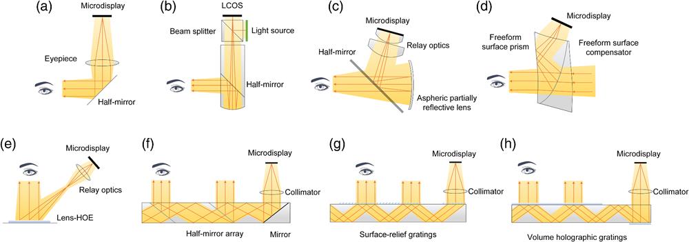
    Fig. 1. Current mainstream AR display solutions. (a) Schematic of a simple conventional optics solution comprising an eyepiece and a half-mirror. The eyepiece is used to collimate image-bearing light from the microdisplay, and the half-mirror is used to combine the virtual image with the real-world scene. (b) Schematic of a conventional optics solution using an embedded half-mirror. A half-mirror is embedded inside the glass slab, which has a curved end to reflect and collimate the incoming light. The virtual images are generated by a liquid crystal on silicon (LCOS) panel with a light source. (c) Schematic of the birdbath conventional optics solution. The relay lenses and the aspheric partially reflective lens are used to collimate light from the microdisplay. (d) Schematic of a typical freeform optics solution comprising an FFS prism and an FFS compensator. The FFS prism can collimate light coming from microdisplay, whereas the FFS compensator is designed to correct the ambient view distortion caused by the FFS prism. (e) Schematic of a holographic optics solution using a lens-HOE as the combiner. The lens-HOE can collimate the relayed image and direct it into the eye. (f)–(h) Schematics of three types of optical waveguide solutions, respectively, using (f) a half-mirror array, (g) surface-relief gratings, and (h) volume holographic gratings as couplers. In these designs, the couplers on the two ends of the transparent waveguide can direct image-bearing light into the waveguide and then extract it out of waveguide, respectively, such that the waveguide system can convey the images from microdisplay to the eye.
    Schematic of metasurface-enabled beam steering. A phase gradient along the x axis is implemented by an array of size-varying meta-atoms and imparted on a normally incident beam. Consequently, the beam bends along the z axis upon transmission. The solid and dashed yellow arrows, respectively, denote the propagation directions of the incident and transmitted beams.
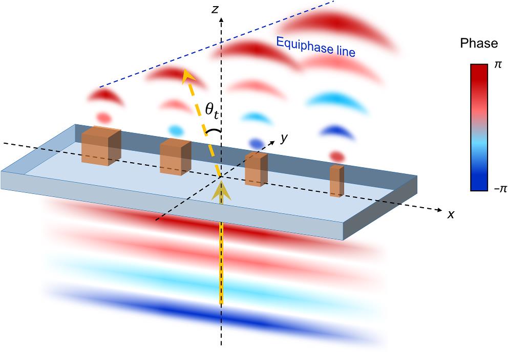
    Fig. 2. Schematic of metasurface-enabled beam steering. A phase gradient along the x axis is implemented by an array of size-varying meta-atoms and imparted on a normally incident beam. Consequently, the beam bends along the z axis upon transmission. The solid and dashed yellow arrows, respectively, denote the propagation directions of the incident and transmitted beams.
    Schematic illustrations of representative phase modulation mechanisms and the associated meta-atom designs. (a) Resonant phase using V-shaped metallic nanoantenna. When an x-polarized light is incident onto the nanoantenna and excites its resonant modes, the converted cross-polarized (y-polarized) transmitted light will experience a nontrivial phase-shift modulation. The resonant condition as well as the induced phase-shift modulation can be tuned via adjusting the opening angle and the arm lengths of the V-shaped nanoantenna. (b) Geometric phase using anisotropic nanorod. When a circularly polarized light is incident onto an array of anisotropic nanorods with the same size but different in-plane orientation angles (α), the converted cross-circularly polarized component of the transmitted light will be imparted a phase-shift modulation that is twice the nanorod orientation angle α. In order to enhance the polarization conversion efficiency and maximize the amount of properly modulated transmission component, meta-atoms with half-wave plate responses are commonly employed. (c) Propagation phase using dielectric nanopillar. When an incident light propagates through the dielectric nanopillar, it acts as a truncated dielectric waveguide with top and bottom interfaces of low reflectivity and imparts a phase-shift modulation onto the transmitted light. Propagation phase can be tuned by various factors including the nanopillar’s height, cross-sectional dimension, lattice spacing, as well as constituent material. Depending on whether the nanopillar is isotropic or anisotropic, the imparted phase shift can be either polarization-independent or polarization-dependent. (d) Combined use of geometric phase and propagation phase. By simultaneously adjusting the nanopillar’s cross-sectional dimension and orientation angle, independent phase-shift modulation can be imparted onto two arbitrary orthogonal polarization states. (e) Detour phase using meta-atom design consisting of a bottom metallic reflective layer, a dielectric gap layer, and a metallic nanorod on top. For an oblique-incident light with polarization direction parallel to the long axis of the nanorod, localized surface plasmon resonance is predominantly excited and phase-shift modulation is imparted onto the first-order diffracted light having the same SOP. Detour phase can be tuned via adjusting the nanorod displacement within its unit cell. (f) ET phase using meta-atom design consisting of a bottom metallic reflective layer, a dielectric gap layer, and a pair of near-field-coupled nanorods on top. By adjusting the meta-atom structural parameters to encircle an optical singularity following an arbitrarily closed trajectory in the parameter space, a topologically protected full 2π phase modulation is applied onto the circularly polarized reflected light of opposite handedness. (g) Quasi-BIC geometric phase using meta-atom design comprising a pair of perpendicularly orientated anisotropic nanoholes based on high-refractive-index dielectric material. The asymmetrical geometry of the nanoholes is designed to perturbate the symmetry-protected BIC and induce free-space light radiation. Working around its resonant frequency, the meta-atom can flip the handedness of an incident circularly polarized light and impart a phase-shift modulation four times the nanoantenna orientation angle α onto the converted cross-polarized transmitted light.
    Fig. 3. Schematic illustrations of representative phase modulation mechanisms and the associated meta-atom designs. (a) Resonant phase using V-shaped metallic nanoantenna. When an x-polarized light is incident onto the nanoantenna and excites its resonant modes, the converted cross-polarized (y-polarized) transmitted light will experience a nontrivial phase-shift modulation. The resonant condition as well as the induced phase-shift modulation can be tuned via adjusting the opening angle and the arm lengths of the V-shaped nanoantenna. (b) Geometric phase using anisotropic nanorod. When a circularly polarized light is incident onto an array of anisotropic nanorods with the same size but different in-plane orientation angles (α), the converted cross-circularly polarized component of the transmitted light will be imparted a phase-shift modulation that is twice the nanorod orientation angle α. In order to enhance the polarization conversion efficiency and maximize the amount of properly modulated transmission component, meta-atoms with half-wave plate responses are commonly employed. (c) Propagation phase using dielectric nanopillar. When an incident light propagates through the dielectric nanopillar, it acts as a truncated dielectric waveguide with top and bottom interfaces of low reflectivity and imparts a phase-shift modulation onto the transmitted light. Propagation phase can be tuned by various factors including the nanopillar’s height, cross-sectional dimension, lattice spacing, as well as constituent material. Depending on whether the nanopillar is isotropic or anisotropic, the imparted phase shift can be either polarization-independent or polarization-dependent. (d) Combined use of geometric phase and propagation phase. By simultaneously adjusting the nanopillar’s cross-sectional dimension and orientation angle, independent phase-shift modulation can be imparted onto two arbitrary orthogonal polarization states. (e) Detour phase using meta-atom design consisting of a bottom metallic reflective layer, a dielectric gap layer, and a metallic nanorod on top. For an oblique-incident light with polarization direction parallel to the long axis of the nanorod, localized surface plasmon resonance is predominantly excited and phase-shift modulation is imparted onto the first-order diffracted light having the same SOP. Detour phase can be tuned via adjusting the nanorod displacement within its unit cell. (f) ET phase using meta-atom design consisting of a bottom metallic reflective layer, a dielectric gap layer, and a pair of near-field-coupled nanorods on top. By adjusting the meta-atom structural parameters to encircle an optical singularity following an arbitrarily closed trajectory in the parameter space, a topologically protected full 2π phase modulation is applied onto the circularly polarized reflected light of opposite handedness. (g) Quasi-BIC geometric phase using meta-atom design comprising a pair of perpendicularly orientated anisotropic nanoholes based on high-refractive-index dielectric material. The asymmetrical geometry of the nanoholes is designed to perturbate the symmetry-protected BIC and induce free-space light radiation. Working around its resonant frequency, the meta-atom can flip the handedness of an incident circularly polarized light and impart a phase-shift modulation four times the nanoantenna orientation angle α onto the converted cross-polarized transmitted light.
    Nonconventional fabrication processes for AR-display-orientated metasurfaces. (a) Damascene lithography. Left panel: schematic illustration of a typical damascene lithography process for HfO2-based metasurface fabrication. It starts by spin-coating an e-beam resist layer of the same height as the designed nanostructure onto a fused silica substrate. E-beam lithography is used to pattern the resist layer and creates a resist template. The metasurface constituent material (HfO2 in this case) is subsequently deposited onto the patterned resist template through low temperature ALD, providing a complete filling of the patterns as well as substantial over-coating of the resist, yielding a quasi-planar top surface. Following that, the overcoated quasi-planar layer is back-etched to expose the underlying resist and the top of the nanostructures. Finally, the remaining resist is removed by solvent soaking, yielding high-aspect-ratio structures with smooth and straight sidewall profiles. Right panel: scanning electron micrograph (SEM) of a fabricated HfO2 metalens consisting of arrays of circular nanopillars with spatially varying diameters. Scale bar: 300 nm. Inset: optical microscope image of the same sample. Scale bar: 100 μm. Adapted with permission from Ref. 72. Copyright 2020, Nature Publishing Group. (b) Nanoimprint lithography. Left panel: schematic illustration of a typical NIL process for fabricating metasurfaces made of UV curable resin, which contains TiO2 nanoparticles for refractive index enhancement. It starts by replicating a soft polydimethylsiloxane (PDMS) mold from a hard Si master mold. The bi-layer PDMS mold, consisting of a hard PDMS (h-PDMS) structured layer and a regular PDMS substrate layer, is employed to ensure high patterning resolution. Then the PDMS mold is used to pattern the UV-curable resin layer through NIL, generating the target metasurface pattern. The refractive index of the resin can be tuned (from ∼1.53 to ∼1.94) by adjusting the weight ratio of TiO2 nanoparticles. Right panel: SEM of an imprinted resin-based metalens consisting of arrays of rectangular nanorods with spatially varying orientation angles. Scale bar: 1 μm. Inset: optical microscope image of the same sample. Scale bar: 100 μm. Adapted with permission from Ref. 122. Copyright 2020, Nature Publishing Group.
    Fig. 4. Nonconventional fabrication processes for AR-display-orientated metasurfaces. (a) Damascene lithography. Left panel: schematic illustration of a typical damascene lithography process for HfO2-based metasurface fabrication. It starts by spin-coating an e-beam resist layer of the same height as the designed nanostructure onto a fused silica substrate. E-beam lithography is used to pattern the resist layer and creates a resist template. The metasurface constituent material (HfO2 in this case) is subsequently deposited onto the patterned resist template through low temperature ALD, providing a complete filling of the patterns as well as substantial over-coating of the resist, yielding a quasi-planar top surface. Following that, the overcoated quasi-planar layer is back-etched to expose the underlying resist and the top of the nanostructures. Finally, the remaining resist is removed by solvent soaking, yielding high-aspect-ratio structures with smooth and straight sidewall profiles. Right panel: scanning electron micrograph (SEM) of a fabricated HfO2 metalens consisting of arrays of circular nanopillars with spatially varying diameters. Scale bar: 300 nm. Inset: optical microscope image of the same sample. Scale bar: 100  μm. Adapted with permission from Ref. 72. Copyright 2020, Nature Publishing Group. (b) Nanoimprint lithography. Left panel: schematic illustration of a typical NIL process for fabricating metasurfaces made of UV curable resin, which contains TiO2 nanoparticles for refractive index enhancement. It starts by replicating a soft polydimethylsiloxane (PDMS) mold from a hard Si master mold. The bi-layer PDMS mold, consisting of a hard PDMS (h-PDMS) structured layer and a regular PDMS substrate layer, is employed to ensure high patterning resolution. Then the PDMS mold is used to pattern the UV-curable resin layer through NIL, generating the target metasurface pattern. The refractive index of the resin can be tuned (from 1.53 to 1.94) by adjusting the weight ratio of TiO2 nanoparticles. Right panel: SEM of an imprinted resin-based metalens consisting of arrays of rectangular nanorods with spatially varying orientation angles. Scale bar: 1  μm. Inset: optical microscope image of the same sample. Scale bar: 100  μm. Adapted with permission from Ref. 122. Copyright 2020, Nature Publishing Group.
    Conceptual schematic of a waveguide-based AR display system utilizing three types of metadevices. Target images are generated by the metahologram, and then the image-bearing rays are collimated by the metalens. The collimated rays are coupled into and out of the waveguide by the metacouplers located at both ends and ultimately projected onto the human eye.
    Fig. 5. Conceptual schematic of a waveguide-based AR display system utilizing three types of metadevices. Target images are generated by the metahologram, and then the image-bearing rays are collimated by the metalens. The collimated rays are coupled into and out of the waveguide by the metacouplers located at both ends and ultimately projected onto the human eye.
    Visible metalenses and their imaging applications. (a) Optical microscope image and (b) SEM of a visible geometric-phase-based metalens using rectangular TiO2 nanopillars. Scale bars: (a) 40 μm and (b) 300 nm. (c) Right panel: image of a 1951 USAF resolution test chart formed by the metalens operating at λ0=532 nm. Scale bar: 40 μm. Left panel: four images of the highlighted region formed by the same metalens with illumination wavelengths of 480, 530, 590, and 620 nm, respectively. Thanks to the broadband response of geometric phase modulation, the device maintains decent focusing capability across the whole visible region and these micrometer-sized lines in the highlighted region can be clearly resolved in all cases. Scale bar: 5 μm. Adapted with permission from Ref. 67. Copyright 2016, American Association for the Advancement of Science (AAAS). (d) Schematic illustration and (e) SEM of a near-unity-NA (0.99) metalens composed of circular Si nanopillars with spatially varying radii operating at 715 nm. Scale bar: 5 μm. (f) Normalized measured intensity distribution around the metalens focal point along the x axis as a function of the distance to the lens. The metalens has a diameter of 600 μm and focuses light at a distance between 42 and 47 μm, corresponding to an NA of 0.99. Reproduced with permission from Ref. 109. Copyright 2018, American Chemical Society. (g) Schematic illustration of a geometric-phase-based TiO2 metalens for chiral imaging, which focuses incoming light onto different points on the same focal plane, depending on its handedness. [This figure is plotted based on Fig. (d) of the review summary of Ref. 140]. (h) SEM of the metalens, composed of two sets of rectangular nanopillars (blue and green false-colored), which are spatially interleaved and, respectively, responsible for imparting the required phase modulation profiles to focus RCP and LCP incident light. Scale bar: 600 nm. (i) Imaging of a Chrysina gloriosa beetle with the chiral metalens at λ0≈532 nm. The two images are, respectively, formed by focusing the LCP and RCP reflected light from the beetle, whose exoskeleton exhibits strong CD and reflects a larger amount of LCP light. Adapted with permission Ref. 92. Copyright 2016, American Chemical Society. (j) Schematic illustration of edge-detection imaging using a spiral metalens. (k) Bright-field (upper panel, taken with a 50× objective lens) and edge-enhanced (lower panel, taken with the spiral metalens) images of erythrocytes at discrete illumination wavelengths of 497, 532, 580, and 633 nm, where the edge-enhanced images show discernible erythrocyte boundaries with a high contrast. Scale bars: 10 μm. Reproduced with permission from Ref. 144. Copyright 2018, Wiley-VCH.
    Fig. 6. Visible metalenses and their imaging applications. (a) Optical microscope image and (b) SEM of a visible geometric-phase-based metalens using rectangular TiO2 nanopillars. Scale bars: (a) 40  μm and (b) 300 nm. (c) Right panel: image of a 1951 USAF resolution test chart formed by the metalens operating at λ0=532  nm. Scale bar: 40  μm. Left panel: four images of the highlighted region formed by the same metalens with illumination wavelengths of 480, 530, 590, and 620 nm, respectively. Thanks to the broadband response of geometric phase modulation, the device maintains decent focusing capability across the whole visible region and these micrometer-sized lines in the highlighted region can be clearly resolved in all cases. Scale bar: 5  μm. Adapted with permission from Ref. 67. Copyright 2016, American Association for the Advancement of Science (AAAS). (d) Schematic illustration and (e) SEM of a near-unity-NA (0.99) metalens composed of circular Si nanopillars with spatially varying radii operating at 715 nm. Scale bar: 5  μm. (f) Normalized measured intensity distribution around the metalens focal point along the x axis as a function of the distance to the lens. The metalens has a diameter of 600  μm and focuses light at a distance between 42 and 47  μm, corresponding to an NA of 0.99. Reproduced with permission from Ref. 109. Copyright 2018, American Chemical Society. (g) Schematic illustration of a geometric-phase-based TiO2 metalens for chiral imaging, which focuses incoming light onto different points on the same focal plane, depending on its handedness. [This figure is plotted based on Fig. (d) of the review summary of Ref. 140]. (h) SEM of the metalens, composed of two sets of rectangular nanopillars (blue and green false-colored), which are spatially interleaved and, respectively, responsible for imparting the required phase modulation profiles to focus RCP and LCP incident light. Scale bar: 600 nm. (i) Imaging of a Chrysina gloriosa beetle with the chiral metalens at λ0532  nm. The two images are, respectively, formed by focusing the LCP and RCP reflected light from the beetle, whose exoskeleton exhibits strong CD and reflects a larger amount of LCP light. Adapted with permission Ref. 92. Copyright 2016, American Chemical Society. (j) Schematic illustration of edge-detection imaging using a spiral metalens. (k) Bright-field (upper panel, taken with a 50× objective lens) and edge-enhanced (lower panel, taken with the spiral metalens) images of erythrocytes at discrete illumination wavelengths of 497, 532, 580, and 633 nm, where the edge-enhanced images show discernible erythrocyte boundaries with a high contrast. Scale bars: 10  μm. Reproduced with permission from Ref. 144. Copyright 2018, Wiley-VCH.
    Ray-tracing schematic of a geometric-phase-based metalens under different illumination wavelengths. The metalens is designed to operate at free-space wavelength λ0 with a focal length of f0. Incident light of different free-space wavelengths exhibits different types of spherical aberrations, depending on whether their wavelength is longer or shorter than the device’s design wavelength. For an incident light whose free-space wavelength deviates from the device’s designed one, intersection points between different light rays with the metalens’ optical axis exhibit dependence on the ray’s incident position.
    Fig. 7. Ray-tracing schematic of a geometric-phase-based metalens under different illumination wavelengths. The metalens is designed to operate at free-space wavelength λ0 with a focal length of f0. Incident light of different free-space wavelengths exhibits different types of spherical aberrations, depending on whether their wavelength is longer or shorter than the device’s design wavelength. For an incident light whose free-space wavelength deviates from the device’s designed one, intersection points between different light rays with the metalens’ optical axis exhibit dependence on the ray’s incident position.
    Broadband achromatic metalenses. (a) Ray-tracing schematic of a broadband achromatic metalens. φ(r,ω) is the required spatial- and angular-frequency-dependent phase-shift modulation for achromatic focusing over the target operation band. (b) Schematic of a broadband achromatic metalens unit cell comprising two coupled rectangular TiO2 nanopillars. (c) The associated SEM of the metalens. Scale bar: 500 nm. (d) Measured intensity distributions of transmitted light along z axis at different illumination wavelengths from 470 to 670 nm. Reproduced with permission from Ref. 155. Copyright 2018, Nature Publishing Group. (e) Optical microscope image of a GaN-based broadband achromatic metalens. Scale bar: 10 μm. (f) SEMs showing details of different areas of the achromatic metalens consisting of rectangular GaN nanopillars and nanoholes. Scale bar: 500 nm. (g) A full-color image of Erithacus rubecula formed by the broadband achromatic metalens. Reproduced with permission from Ref. 95. Copyright 2018, Nature Publishing Group. (h) Calculated phase and dispersion of fourfold symmetric, a-Si nanopillars of the same height but different cross-sectional shapes. (i) SEM of the polarization-independent broadband achromatic metalens. Scale bar: 5 μm. (j) Measured intensity distributions of transmitted light along z axis at different illumination wavelengths from 1200 to 1650 nm. Adapted with permission Ref. 156. Copyright 2018, Nature Publishing Group.
    Fig. 8. Broadband achromatic metalenses. (a) Ray-tracing schematic of a broadband achromatic metalens. φ(r,ω) is the required spatial- and angular-frequency-dependent phase-shift modulation for achromatic focusing over the target operation band. (b) Schematic of a broadband achromatic metalens unit cell comprising two coupled rectangular TiO2 nanopillars. (c) The associated SEM of the metalens. Scale bar: 500 nm. (d) Measured intensity distributions of transmitted light along z axis at different illumination wavelengths from 470 to 670 nm. Reproduced with permission from Ref. 155. Copyright 2018, Nature Publishing Group. (e) Optical microscope image of a GaN-based broadband achromatic metalens. Scale bar: 10  μm. (f) SEMs showing details of different areas of the achromatic metalens consisting of rectangular GaN nanopillars and nanoholes. Scale bar: 500  nm. (g) A full-color image of Erithacus rubecula formed by the broadband achromatic metalens. Reproduced with permission from Ref. 95. Copyright 2018, Nature Publishing Group. (h) Calculated phase and dispersion of fourfold symmetric, a-Si nanopillars of the same height but different cross-sectional shapes. (i) SEM of the polarization-independent broadband achromatic metalens. Scale bar: 5  μm. (j) Measured intensity distributions of transmitted light along z axis at different illumination wavelengths from 1200 to 1650 nm. Adapted with permission Ref. 156. Copyright 2018, Nature Publishing Group.
    Metalens-based AR displays. (a) Schematic of a near-eye display system composed of a microdisplay, a 4-f relay system, a beam splitter, a stack of dichroic mirrors, several circular polarizers, and a 20-mm-diameter, geometric-phase-based Si metalens. Virtual RGB images from the microdisplay are, respectively, displayed near the corresponding focal planes of the metalens with the proper arrangement of dichroic mirrors. Inset: photograph and SEM of the metalens. Scale bar: 2 cm (in photograph) and 500 nm (in SEM). (b) A photo of virtual color images displayed over a real-world scene. Adapted with permission from Ref. 119. Copyright 2018, Nature Publishing Group. (c) Schematic of a color AR display system employing a multiwavelength achromatic TiO2 metalens and an optical combiner. (d) SEM of the designed multiwavelength achromatic metalens, which consists of coupled rectangular TiO2 nanopillars with spatially varying geometries and orientations. Scale bar: 1 μm. (e) AR display result with floating virtual images of three-color RGB letters in a real-world scene. Reproduced with permission from Ref. 152. Copyright 2021, AAAS. (f) Schematic of a Maxwellian-view-based AR display system using a geometric-phase-based, reflection-type Si metalens. (g) Demonstration of single-color AR imaging under red (λ0=633 nm) laser illumination. The AR image is always clear when the camera is focused on the dial at 150 mm (left panel) and on the puppet at 600 mm (right panel), respectively. Reproduced with permission from Ref. 171. Copyright 2022, Springer Publishing.
    Fig. 9. Metalens-based AR displays. (a) Schematic of a near-eye display system composed of a microdisplay, a 4-f relay system, a beam splitter, a stack of dichroic mirrors, several circular polarizers, and a 20-mm-diameter, geometric-phase-based Si metalens. Virtual RGB images from the microdisplay are, respectively, displayed near the corresponding focal planes of the metalens with the proper arrangement of dichroic mirrors. Inset: photograph and SEM of the metalens. Scale bar: 2 cm (in photograph) and 500 nm (in SEM). (b) A photo of virtual color images displayed over a real-world scene. Adapted with permission from Ref. 119. Copyright 2018, Nature Publishing Group. (c) Schematic of a color AR display system employing a multiwavelength achromatic TiO2 metalens and an optical combiner. (d) SEM of the designed multiwavelength achromatic metalens, which consists of coupled rectangular TiO2 nanopillars with spatially varying geometries and orientations. Scale bar: 1  μm. (e) AR display result with floating virtual images of three-color RGB letters in a real-world scene. Reproduced with permission from Ref. 152. Copyright 2021, AAAS. (f) Schematic of a Maxwellian-view-based AR display system using a geometric-phase-based, reflection-type Si metalens. (g) Demonstration of single-color AR imaging under red (λ0=633  nm) laser illumination. The AR image is always clear when the camera is focused on the dial at 150 mm (left panel) and on the puppet at 600 mm (right panel), respectively. Reproduced with permission from Ref. 171. Copyright 2022, Springer Publishing.
    Metacouplers for guided light engineering. (a) Schematic of a polarization-dependent directional metagrating in-coupler. The metacoupler, consisting of rectangular Si nanopillars with spatially varying sizes and orientation angles, can directionally couple an x-polarized incident light to a right-propagating fundamental transverse magnetic mode (TM00), and a y-polarized incident light into a left-propagating fundamental transverse electric mode (TE00). Reproduced with permission from Ref. 174. Copyright 2020, Chinese Laser Press. (b) Schematic of a directional metagrating out-coupler. The metacoupler is made of an array of rectangular meta-atoms having a metal/dielectric/metal sandwiched structure and offers a phase gradient ∂Δφ(x)/∂x along the positive x direction. Simulated electric-field distributions around the metacoupler region, respectively, for a forward-propagating (along positive x direction; upper panel) and a backward-propagating (along negative x direction; lower panel) guided light illustrate the directional out-coupling effect. A forward-propagating guided light is launched into free space at an angle θ=arcsin[neffn0+∂Δφ(x)k0n0∂x] by the metacoupler, whereas a backward-propagating guided light ends up having a transverse wave vector (kx) exceeding the largest supportable one in free space and gets confined to the device surface. Adapted with permission from Ref. 175. Copyright 2020, AAAS. (c) Schematic of a metacoupler-assisted asymmetric waveguide mode conversion process. The metacoupler consists of Au microrods with the same orientation angle but different lengths. Along the forward propagation direction, an incident fundamental waveguide mode TE00 can be converted into a higher-order waveguide mode TE10; whereas along the backward propagation direction, the same incident mode is blocked. Adapted with permission from Ref. 176. Copyright 2019, American Chemical Society. (d) Schematic of switchable off-waveguide focusing facilitated by a metacoupler atop a Si waveguide. The metacoupler is excited by the guided mode inside the Si waveguide and creates focusing emission in free space. The focused spot can be switched between two positions depending on the excitation direction (indicated by the green and red arrows). Inset shows the layout of the meta-atom unit cell, composed of a circular a-Si nanopillar having a SiO2 cover layer. The nanopillar is evanescently coupled to the underneath Si waveguide through a SiO2 interlayer. Reproduced with permission from Ref. 181. Copyright 2022, De Gruyter.
    Fig. 10. Metacouplers for guided light engineering. (a) Schematic of a polarization-dependent directional metagrating in-coupler. The metacoupler, consisting of rectangular Si nanopillars with spatially varying sizes and orientation angles, can directionally couple an x-polarized incident light to a right-propagating fundamental transverse magnetic mode (TM00), and a y-polarized incident light into a left-propagating fundamental transverse electric mode (TE00). Reproduced with permission from Ref. 174. Copyright 2020, Chinese Laser Press. (b) Schematic of a directional metagrating out-coupler. The metacoupler is made of an array of rectangular meta-atoms having a metal/dielectric/metal sandwiched structure and offers a phase gradient Δφ(x)/x along the positive x direction. Simulated electric-field distributions around the metacoupler region, respectively, for a forward-propagating (along positive x direction; upper panel) and a backward-propagating (along negative x direction; lower panel) guided light illustrate the directional out-coupling effect. A forward-propagating guided light is launched into free space at an angle θ=arcsin[neffn0+Δφ(x)k0n0x] by the metacoupler, whereas a backward-propagating guided light ends up having a transverse wave vector (kx) exceeding the largest supportable one in free space and gets confined to the device surface. Adapted with permission from Ref. 175. Copyright 2020, AAAS. (c) Schematic of a metacoupler-assisted asymmetric waveguide mode conversion process. The metacoupler consists of Au microrods with the same orientation angle but different lengths. Along the forward propagation direction, an incident fundamental waveguide mode TE00 can be converted into a higher-order waveguide mode TE10; whereas along the backward propagation direction, the same incident mode is blocked. Adapted with permission from Ref. 176. Copyright 2019, American Chemical Society. (d) Schematic of switchable off-waveguide focusing facilitated by a metacoupler atop a Si waveguide. The metacoupler is excited by the guided mode inside the Si waveguide and creates focusing emission in free space. The focused spot can be switched between two positions depending on the excitation direction (indicated by the green and red arrows). Inset shows the layout of the meta-atom unit cell, composed of a circular a-Si nanopillar having a SiO2 cover layer. The nanopillar is evanescently coupled to the underneath Si waveguide through a SiO2 interlayer. Reproduced with permission from Ref. 181. Copyright 2022, De Gruyter.
    Waveguide AR displays using polarization-sensitive metagrating couplers. (a) Schematic of an FOV-enhanced waveguide display system, whose major parts include a microdisplay, two orthogonal linear polarizers covering the left and right halves of the display, a collimator, and a pair of in-coupler and out-coupler on the waveguide slab surface. Image-bearing light rays coming from the left (TE-polarized) and right (TM-polarized) parts of the polarizer-covered microdisplay, each of which corresponds to one half of the enlarged FOV, are deflected into the waveguide by the in-coupler and subsequently extracted by the metagrating out-coupler. (b) Schematic of the metagrating out-coupler. The out-coupler comprises two types of polarization-selective spatially interleaved metagratings having different slanted angles, heights, periods, and refractive indices. Each metagrating is designed to out-couple guided light of a given SOP (TE or TM), whereas back-reflect light of the orthogonal SOP (TM or TE) to avoid crosstalk between the two polarization channels. Reproduced with permission from Ref. 182. Copyright 2018, Society of Photo-Optical Instrumentation Engineers (SPIE). (c) Schematic of a stereo waveguide 3D display utilizing a polarization-multiplexed metagrating in-coupler. Incident beams of opposite circular polarization states carrying stereoscopic images are steered by the metagrating in-coupler to opposite propagation directions in the flat glass waveguide and are subsequently extracted by two surface-relief grating out-couplers for stereo 3D vision formation. (d) Upper panel: SEM of the geometric-phase-based spin-multiplexed metagrating in-coupler, consisting of arrays of elliptical Au nanobars. Scale bar: 500 nm. Lower panel: SEM of the UV-curable resin based out-coupling grating fabricated by NIL. Scale bar: 2 μm. (e) Two AR images at the eye boxes of the constructed display system, respectively, captured by eye-mimicking cameras. Two stereoscopic virtual images (two perspective views of an octahedron) overlapped on an ambient scene can be received independently with high fidelity and negligible crosstalk. Reproduced with permission from Ref. 183. Copyright 2021, American Chemical Society.
    Fig. 11. Waveguide AR displays using polarization-sensitive metagrating couplers. (a) Schematic of an FOV-enhanced waveguide display system, whose major parts include a microdisplay, two orthogonal linear polarizers covering the left and right halves of the display, a collimator, and a pair of in-coupler and out-coupler on the waveguide slab surface. Image-bearing light rays coming from the left (TE-polarized) and right (TM-polarized) parts of the polarizer-covered microdisplay, each of which corresponds to one half of the enlarged FOV, are deflected into the waveguide by the in-coupler and subsequently extracted by the metagrating out-coupler. (b) Schematic of the metagrating out-coupler. The out-coupler comprises two types of polarization-selective spatially interleaved metagratings having different slanted angles, heights, periods, and refractive indices. Each metagrating is designed to out-couple guided light of a given SOP (TE or TM), whereas back-reflect light of the orthogonal SOP (TM or TE) to avoid crosstalk between the two polarization channels. Reproduced with permission from Ref. 182. Copyright 2018, Society of Photo-Optical Instrumentation Engineers (SPIE). (c) Schematic of a stereo waveguide 3D display utilizing a polarization-multiplexed metagrating in-coupler. Incident beams of opposite circular polarization states carrying stereoscopic images are steered by the metagrating in-coupler to opposite propagation directions in the flat glass waveguide and are subsequently extracted by two surface-relief grating out-couplers for stereo 3D vision formation. (d) Upper panel: SEM of the geometric-phase-based spin-multiplexed metagrating in-coupler, consisting of arrays of elliptical Au nanobars. Scale bar: 500 nm. Lower panel: SEM of the UV-curable resin based out-coupling grating fabricated by NIL. Scale bar: 2  μm. (e) Two AR images at the eye boxes of the constructed display system, respectively, captured by eye-mimicking cameras. Two stereoscopic virtual images (two perspective views of an octahedron) overlapped on an ambient scene can be received independently with high fidelity and negligible crosstalk. Reproduced with permission from Ref. 183. Copyright 2021, American Chemical Society.
    Waveguide AR displays using achromatic metagrating couplers. (a) Concept of an achromatic metagrating decorated waveguide display. Co-propagating RGB light (indicated by the white arrows) enters the waveguide through the metagrating in-coupler with the same TIR angle, bounces back and forth inside the waveguide slab, and finally exits the waveguide through the metagrating out-coupler with the same exit angle. Both couplers are in the form of stacked grating layers, where each layer consists of TiO2 and SiO2 nanoridges. (b) Electromagnetic full-wave simulation showing achromatic coupling functions for both the in-coupling (upper panel) and out-coupling (lower panel) processes. The metagrating in-coupler and out-coupler are, respectively, designed to have a nine-layer and six-layer structure. Adapted with permission from Ref. 186. Copyright 2021, Optica Publishing Group. (c) Ray-tracing schematic of the in-coupling and out-coupling processes of RGB light in a planar waveguide using multilayer reflective achromatic metagrating couplers. (d) Left panel: simulation scheme of the metagrating in-coupler consisting of three layers of metallic circular nanodisks of different sizes. The disks in different layers are, respectively, made of Al, Ag, and Au from top to the bottom, and they are spaced with a 200-nm-thick SiO2 buffer layer to avoid strong coupling effect between them. Right panel: simulated transmission spectrum of the multilayer reflective achromatic metagrating coupler, showing three dips at the design wavelengths λ0=450, 550, and 650 nm. Reproduced with permission from Ref. 188. Copyright 2019, SPIE.
    Fig. 12. Waveguide AR displays using achromatic metagrating couplers. (a) Concept of an achromatic metagrating decorated waveguide display. Co-propagating RGB light (indicated by the white arrows) enters the waveguide through the metagrating in-coupler with the same TIR angle, bounces back and forth inside the waveguide slab, and finally exits the waveguide through the metagrating out-coupler with the same exit angle. Both couplers are in the form of stacked grating layers, where each layer consists of TiO2 and SiO2 nanoridges. (b) Electromagnetic full-wave simulation showing achromatic coupling functions for both the in-coupling (upper panel) and out-coupling (lower panel) processes. The metagrating in-coupler and out-coupler are, respectively, designed to have a nine-layer and six-layer structure. Adapted with permission from Ref. 186. Copyright 2021, Optica Publishing Group. (c) Ray-tracing schematic of the in-coupling and out-coupling processes of RGB light in a planar waveguide using multilayer reflective achromatic metagrating couplers. (d) Left panel: simulation scheme of the metagrating in-coupler consisting of three layers of metallic circular nanodisks of different sizes. The disks in different layers are, respectively, made of Al, Ag, and Au from top to the bottom, and they are spaced with a 200-nm-thick SiO2 buffer layer to avoid strong coupling effect between them. Right panel: simulated transmission spectrum of the multilayer reflective achromatic metagrating coupler, showing three dips at the design wavelengths λ0=450, 550, and 650 nm. Reproduced with permission from Ref. 188. Copyright 2019, SPIE.
    Schematic of the modulated light propagation process from the hologram plane to the image plane.
    Fig. 13. Schematic of the modulated light propagation process from the hologram plane to the image plane.
    Metaholograms based on three types of modulation mechanisms: (a), (b) phase-only modulation, (c), (d) amplitude-only modulation, and (e), (f) complex-amplitude modulation. (a) Schematic illustration of a geometric-phase-based, polarization-dependent metahologram consisting of rectangular Au nanobars with spatially varying orientation angles. The metahologram works in the Fresnel diffraction region and is designed to project a 3D image under circularly polarized illumination at λ0=810 nm. Reproduced with permission from Ref. 208. Copyright 2013, Nature Publishing Group. (b) Left panel: schematic illustration of a propagation-phase-based, polarization-independent metahologram in the UV consisting of circular HfO2 nanopillars with spatially varying diameters. Right panel: measured holographic images in the z=40 mm plane, which are projected by three Fraunhofer-diffraction-region metaholograms, respectively, designed at λ0=364, 325, and 266 nm. Reproduced with permission from Ref. 72. Copyright 2020, Nature Publishing Group. (c) Schematic illustration of a transmission-type amplitude-only metahologram in the visible, consisting of uniformly-sized circular nanoholes. The device exhibits polarization-insensitive holographic projection over a broad bandwidth. Reproduced with permission from Ref. 218. Copyright 2017, Wiley-VCH. (d) Upper panel: schematic of a reflection-type amplitude-only metahologram for polarization-dependent multicolor holographic image projection. The metahologram consists of square grids of different types of Ag nanoparticles. Lower panel: a measured multicolor holographic image containing an overlapped red crest and blue text. Adapted with permission from Ref. 219. Copyright 2014, National Academy of Sciences. (e) Schematic illustration of a complex-amplitude metahologram consisting of V-shaped metallic nanogrooves, whose arm lengths and opening angles are varied to independently adjust the phase and amplitude modulations on a linearly polarized incident light at λ0=676 nm. Adapted with permission from Ref. 209. Copyright 2013, Nature Publishing Group. (f) Left panel: schematic illustration of a complex-amplitude metahologram consisting of X-shaped Si meta-atoms, which operates under circularly polarized illumination in the visible. Right panel: 3D and top views of the X-shaped meta-atom. The meta-atom’s two arms, making angles θ1 and θ2 with the x axis, respectively, impart geometric phase modulations of 2θ1 and 2θ2 onto a circularly polarized incident light. The superposition of the above two independent geometric phase modulations leads to an amplitude modulation of cos(θ2−θ1) and phase modulation of θ2+θ1 for the cross-polarized component of transmitted light. Adapted with permission from Ref. 222. Copyright 2018, Royal Society of Chemistry.
    Fig. 14. Metaholograms based on three types of modulation mechanisms: (a), (b) phase-only modulation, (c), (d) amplitude-only modulation, and (e), (f) complex-amplitude modulation. (a) Schematic illustration of a geometric-phase-based, polarization-dependent metahologram consisting of rectangular Au nanobars with spatially varying orientation angles. The metahologram works in the Fresnel diffraction region and is designed to project a 3D image under circularly polarized illumination at λ0=810  nm. Reproduced with permission from Ref. 208. Copyright 2013, Nature Publishing Group. (b) Left panel: schematic illustration of a propagation-phase-based, polarization-independent metahologram in the UV consisting of circular HfO2 nanopillars with spatially varying diameters. Right panel: measured holographic images in the z=40  mm plane, which are projected by three Fraunhofer-diffraction-region metaholograms, respectively, designed at λ0=364, 325, and 266 nm. Reproduced with permission from Ref. 72. Copyright 2020, Nature Publishing Group. (c) Schematic illustration of a transmission-type amplitude-only metahologram in the visible, consisting of uniformly-sized circular nanoholes. The device exhibits polarization-insensitive holographic projection over a broad bandwidth. Reproduced with permission from Ref. 218. Copyright 2017, Wiley-VCH. (d) Upper panel: schematic of a reflection-type amplitude-only metahologram for polarization-dependent multicolor holographic image projection. The metahologram consists of square grids of different types of Ag nanoparticles. Lower panel: a measured multicolor holographic image containing an overlapped red crest and blue text. Adapted with permission from Ref. 219. Copyright 2014, National Academy of Sciences. (e) Schematic illustration of a complex-amplitude metahologram consisting of V-shaped metallic nanogrooves, whose arm lengths and opening angles are varied to independently adjust the phase and amplitude modulations on a linearly polarized incident light at λ0=676  nm. Adapted with permission from Ref. 209. Copyright 2013, Nature Publishing Group. (f) Left panel: schematic illustration of a complex-amplitude metahologram consisting of X-shaped Si meta-atoms, which operates under circularly polarized illumination in the visible. Right panel: 3D and top views of the X-shaped meta-atom. The meta-atom’s two arms, making angles θ1 and θ2 with the x axis, respectively, impart geometric phase modulations of 2θ1 and 2θ2 onto a circularly polarized incident light. The superposition of the above two independent geometric phase modulations leads to an amplitude modulation of cos(θ2θ1) and phase modulation of θ2+θ1 for the cross-polarized component of transmitted light. Adapted with permission from Ref. 222. Copyright 2018, Royal Society of Chemistry.
    In-plane incidence metaholograms. (a) Schematic of a multicolor waveguide metahologram using ZEP resist as the waveguide material. A 1D grating array is etched on one end of the waveguide to couple the incident RGB light, and a binary metahologram pattern is etched on the other end to modulate as well as out-couple the guided light for multicolor holographic image projection in the far field. Reproduced with permission from Ref. 223. Copyright 2019, Optica Publishing Group. (b) Left panel: schematic of a waveguide metahologram employing an array of MDM rectangular meta-atoms on a Si waveguide. The meta-atoms are designed to have spatially varying side lengths to provide phase modulation on the guided light and create a projected holographic image. Right panel: measured holographic image of letter “A” on the plane 40 μm above the waveguide. Adapted with permission from Ref. 225. Copyright 2022, American Chemical Society. (c) Upper panels: SEM of a plasmonic metahologram, which can selectively project four holographic images depending on the propagating directions of excited SPP waves. Lower panels: four measured holographic images of arrow-shaped points on the plane 40 μm above the metahologram. The pointing direction of the arrow corresponds to the propagation direction of incident SPP wave. Adapted with permission from Ref. 226. Copyright 2017, American Chemical Society. (d) Left panel: SEM of a metallic metahologram with a nanohole surrounded by a series of surrounding ring-shaped nanogrooves. Scale bar: 5 μm. Right panel: measured holographic image “O” on the plane 14.5 μm above the metahologram. Reproduced with permission from Ref. 227. Copyright 2012, Nature Publishing Group.
    Fig. 15. In-plane incidence metaholograms. (a) Schematic of a multicolor waveguide metahologram using ZEP resist as the waveguide material. A 1D grating array is etched on one end of the waveguide to couple the incident RGB light, and a binary metahologram pattern is etched on the other end to modulate as well as out-couple the guided light for multicolor holographic image projection in the far field. Reproduced with permission from Ref. 223. Copyright 2019, Optica Publishing Group. (b) Left panel: schematic of a waveguide metahologram employing an array of MDM rectangular meta-atoms on a Si waveguide. The meta-atoms are designed to have spatially varying side lengths to provide phase modulation on the guided light and create a projected holographic image. Right panel: measured holographic image of letter “A” on the plane 40  μm above the waveguide. Adapted with permission from Ref. 225. Copyright 2022, American Chemical Society. (c) Upper panels: SEM of a plasmonic metahologram, which can selectively project four holographic images depending on the propagating directions of excited SPP waves. Lower panels: four measured holographic images of arrow-shaped points on the plane 40  μm above the metahologram. The pointing direction of the arrow corresponds to the propagation direction of incident SPP wave. Adapted with permission from Ref. 226. Copyright 2017, American Chemical Society. (d) Left panel: SEM of a metallic metahologram with a nanohole surrounded by a series of surrounding ring-shaped nanogrooves. Scale bar: 5  μm. Right panel: measured holographic image “O” on the plane 14.5  μm above the metahologram. Reproduced with permission from Ref. 227. Copyright 2012, Nature Publishing Group.
    Metahologram-based AR displays. (a) Schematic of a 3D AR display system consisting of a laser light source, a metahologram, a half-mirror, and a concave mirror. The projected holographic images by the metahologram are first magnified by the concave mirror and then reflected to viewer’s eyes by the half-mirror. Inset: SEM of the metahologram using Si circular nanodisks with spatially varying diameters. Scale bar: 1 μm. (b) Camera-captured photos of virtual images displayed over a real-world scene. For the left and right photos, the camera is focused at 0.5 m away (2 diopters) and 2 m away (0.5 diopters), respectively. The bottom row displays the enlarged parts of the captured photos, where different 2D holographic images are clearly observed at discrete projection distances. Adapted with permission from Ref. 228. Copyright 2021, Wiley-VCH. (c) Schematic of a holographic Maxwellian-view-based, always-in-focus AR display consisting of a laser source, an optical see-through eyepiece (combination of beam splitter and concave mirror), and a metahologram. (d) Projected virtual images along with the real-world scene captured by a camera, respectively, focused at 0.5 m away (2 diopters) and 2 m away (0.5 diopters). The sharpness of the holographic image remains invariant when the camera focuses at different depths, while that of the near and far reference toys changes. Reproduced with permission from Ref. 229. Copyright 2022, Wiley-VCH. (e) Schematic of a multiplexed on-chip metahologram employing Si meta-atoms on Si3N4 waveguide for RGB color AR display. (f) Captured photos with colored “R,” “G,” and “B” letters superimposing onto the corresponding colored objects. Reproduced with permission from Ref. 230. Copyright 2022, Wiley-VCH.
    Fig. 16. Metahologram-based AR displays. (a) Schematic of a 3D AR display system consisting of a laser light source, a metahologram, a half-mirror, and a concave mirror. The projected holographic images by the metahologram are first magnified by the concave mirror and then reflected to viewer’s eyes by the half-mirror. Inset: SEM of the metahologram using Si circular nanodisks with spatially varying diameters. Scale bar: 1  μm. (b) Camera-captured photos of virtual images displayed over a real-world scene. For the left and right photos, the camera is focused at 0.5 m away (2 diopters) and 2 m away (0.5 diopters), respectively. The bottom row displays the enlarged parts of the captured photos, where different 2D holographic images are clearly observed at discrete projection distances. Adapted with permission from Ref. 228. Copyright 2021, Wiley-VCH. (c) Schematic of a holographic Maxwellian-view-based, always-in-focus AR display consisting of a laser source, an optical see-through eyepiece (combination of beam splitter and concave mirror), and a metahologram. (d) Projected virtual images along with the real-world scene captured by a camera, respectively, focused at 0.5 m away (2 diopters) and 2 m away (0.5 diopters). The sharpness of the holographic image remains invariant when the camera focuses at different depths, while that of the near and far reference toys changes. Reproduced with permission from Ref. 229. Copyright 2022, Wiley-VCH. (e) Schematic of a multiplexed on-chip metahologram employing Si meta-atoms on Si3N4 waveguide for RGB color AR display. (f) Captured photos with colored “R,” “G,” and “B” letters superimposing onto the corresponding colored objects. Reproduced with permission from Ref. 230. Copyright 2022, Wiley-VCH.
    Zeyang Liu, Danyan Wang, Hao Gao, Moxin Li, Huixian Zhou, Cheng Zhang. Metasurface-enabled augmented reality display: a review[J]. Advanced Photonics, 2023, 5(3): 034001
    Download Citation