Huazhong University of Science and Technology, School of Optical and Electronic Information, Wuhan National Laboratory for Optoelectronics, Wuhan, China
Augmented reality (AR) display, which superimposes virtual images on ambient scene, can visually blend the physical world and the digital world and thus opens a new vista for human–machine interaction. AR display is considered as one of the next-generation display technologies and has been drawing huge attention from both academia and industry. Current AR display systems operate based on a combination of various refractive, reflective, and diffractive optical elements, such as lenses, prisms, mirrors, and gratings. Constrained by the underlying physical mechanisms, these conventional elements only provide limited light-field modulation capability and suffer from issues such as bulky volume and considerable dispersion, resulting in large size, severe chromatic aberration, and narrow field of view of the composed AR display system. Recent years have witnessed the emerging of a new type of optical elements—metasurfaces, which are planar arrays of subwavelength electromagnetic structures that feature an ultracompact footprint and flexible light-field modulation capability, and are widely believed to be an enabling tool for overcoming the limitations faced by current AR displays. Here, we aim to provide a comprehensive review on the recent development of metasurface-enabled AR display technology. We first familiarize readers with the fundamentals of AR display, covering its basic working principle, existing conventional-optics-based solutions, as well as the associated pros and cons. We then introduce the concept of optical metasurfaces, emphasizing typical operating mechanisms, and representative phase modulation methods. We elaborate on three kinds of metasurface devices, namely, metalenses, metacouplers, and metaholograms, which have empowered different forms of AR displays. Their physical principles, device designs, and the performance improvement of the associated AR displays are explained in details. In the end, we discuss the existing challenges of metasurface optics for AR display applications and provide our perspective on future research endeavors.
Augmented reality (AR) display superimposes virtual texts or images on top of what a person can already see, enabling connection between the physical world and the digital world.1–7 AR display creates an interwoven experience where digital information alters the user’s perception of the real world and brings new opportunities for highly immersive human–machine interaction. The technology draws huge attention from both academia and industry and has a variety of applications ranging from facilitating decision-making to education and daily entertainment.8–10 During the ongoing global pandemic, the demand for AR display and related technologies has soared as these technologies avoid the need for travel and social contact, and at the same time, provide immersive virtual presence for remote communications.11
The implementation of AR display system relies on wearable see-through near-eye display devices, which project virtual images to the eye(s) while keeping the ambient scene visible. Target virtual images are usually collimated before projection, such that the virtual images can be visually fused with the real distant objects. The key parts of an AR display system include a microdisplay module, a collimator, and a combiner. The collimator is a set of optical elements that collimates images from the microdisplay, and the combiner can combine the virtual images with the ambient scene.
An AR display system is usually characterized by several performance factors, including field of view (FOV), eye box, angular resolution, and focal cue.1,2,8 The FOV of an AR display system refers to the angular extension where the eye can receive the projected virtual image. Human vision’s maximum FOV is around 120 deg for a static eye but can reach up to 160 deg, if eye rolling is considered. The eye box (also referred to as the exit pupil) is the overlapped area among image-bearing rays coming out of the combiner in different spatial angles, and therefore, indicates the spatial range where the user’s eye can see the entire FOV. A larger eye box provides more tolerance to device wiggling during use and accommodates the diversified interpupillary distances of different users. However, due to the conservation of etendue (which equals the product of the source area and the solid angle the area subtends),12,13 there exists a trade-off between the angular range of FOV and the size of the eye box. To increase the system etendue usually requires a larger form factor of the microdisplay module as well as the projection optics, which inevitably compromises the compactness of the AR display system. Angular resolution, defined as the number of pixels within a unit angle, is an important performance factor that measures the sharpness of the projected virtual images. The maximum angular resolution of human eye’s perception is about for central vision and for peripheral vision. A high-resolution microdisplay module is needed to realize high angular resolution across a broad FOV for an AR display system. Focal cue, or depth cue, is a key feature for high-sensation 3D image projection. Incorrect depth cues, resulting from the discrepancy between the depth perceived by the brain and the depth focused on by the individual eye, will lead to the well-known vergence accommodation conflict (VAC), and therefore, are considered a major cause of eye fatigue in long-time use of stereo 3D AR display devices. Relevant approaches to overcome this issue include varifocal displays and multifocal displays,14 which form images in continuous or multiple discrete depth planes, respectively. In addition, the VAC issue can also be mitigated using Maxwellian-view-based displays,15,16 which form always-in-focus images directly on the retina regardless of the crystalline lens’s focus.
Sign up for Advanced Photonics TOC. Get the latest issue of Advanced Photonics delivered right to you!Sign up now
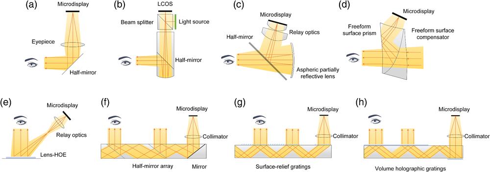
Based on different forms of major employed optical components, current mainstream AR display solutions can be roughly classified into four categories: conventional optics solutions, freeform optics solutions, holographic optics solutions, and optical waveguide solutions. In conventional optics solutions [Figs. 1(a)–1(c)], a series of conventional optical components, such as lenses and mirrors, are employed to construct an off-axis projection system. In its simplest form, an eyepiece is adopted to collimate light rays from the microdisplay module. Then a half-mirror (partially reflective mirror) is used to deflect the collimated light to the eye, and at the same time, allows the ambient light to pass through [Fig. 1(a)]. Such configuration can be reformed by embedding the half-mirror within a glass slab and using its curved end as a reflective collimator [Fig. 1(b)]. This type of design has been adopted by pioneering products, such as Google Glass,17 although it only provides a limited FOV ( in general). The birdbath configuration [Fig. 1(c)], as a more popular conventional optics solution, uses a pair of half-mirror and aspheric partially reflective lens as the combiner.18,19 Such design effectively folds the optical path to improve system compactness, and simultaneously, offers a high degree of design freedom for realizing a broad FOV (). Freeform surface (FFS) prisms are most widely employed in freeform optics solutions, where the systems consist of two major parts: (i) an FFS prism that projects collimated virtual images from the microdisplay module onto the eye and (ii) an FFS compensator cemented on the back of the FFS prism to correct the ambient view distortion caused by the FFS prism [Fig. 1(d)].20–22 Image-bearing light rays are folded twice by total internal reflections (TIRs) on the front and back surfaces of the FFS prism and then exit it as collimated. Such FFS prism solution, characterized by a reduced system size, can offer a broad FOV () and a large eye box (8 mm) at the same time.21 Moreover, several FFS prisms can be pieced together for better display performance, such as larger FOV23 and multifocal image projection.24 However, for daily wear, the constituent FFS optics are still relatively thick (20 to 30 mm). Holographic optics solutions operate based on holographic optical elements (HOEs), which are commonly made of thin photosensitive polymers with a typical thickness of tens of micrometers.25 HOEs can impart wavefront modulation on an incident light according to the recorded interference fringes, and therefore, holographic optics solutions feature reduced form factor and flexible wavefront modulation for both 2D and 3D AR displays.26 In a typical lens-HOE-based AR display system, the virtual image is first delivered by the relay optics onto the focal plane of the lens-HOE, which will collimate the relayed image and direct it into the eye [Fig. 1(e)].27,28 The image source can be a microdisplay or a spatial light modulator (SLM) combined with a laser light source for 2D and 3D image generation, respectively. By employing a lens-array-HOE, 3D AR display can also be realized utilizing integral imaging techniques.29 HOEs typically operate efficiently when their Bragg diffraction conditions are satisfied, and small deviations from such conditions will result in a drastic efficiency decrease. Therefore, the responses of HOEs show high sensitivity to both the angle of incidence and wavelength of the illumination light. Such a characteristic can benefit the transmittance of ambient light for see-through view and enable multiplexed functions.30 Challenges associated with holographic optics solutions include chromatic aberration and oblique astigmatism in imaging, as well as material reliability of the constituted HOEs for long-time use.31
Figure 1.Current mainstream AR display solutions. (a) Schematic of a simple conventional optics solution comprising an eyepiece and a half-mirror. The eyepiece is used to collimate image-bearing light from the microdisplay, and the half-mirror is used to combine the virtual image with the real-world scene. (b) Schematic of a conventional optics solution using an embedded half-mirror. A half-mirror is embedded inside the glass slab, which has a curved end to reflect and collimate the incoming light. The virtual images are generated by a liquid crystal on silicon (LCOS) panel with a light source. (c) Schematic of the birdbath conventional optics solution. The relay lenses and the aspheric partially reflective lens are used to collimate light from the microdisplay. (d) Schematic of a typical freeform optics solution comprising an FFS prism and an FFS compensator. The FFS prism can collimate light coming from microdisplay, whereas the FFS compensator is designed to correct the ambient view distortion caused by the FFS prism. (e) Schematic of a holographic optics solution using a lens-HOE as the combiner. The lens-HOE can collimate the relayed image and direct it into the eye. (f)–(h) Schematics of three types of optical waveguide solutions, respectively, using (f) a half-mirror array, (g) surface-relief gratings, and (h) volume holographic gratings as couplers. In these designs, the couplers on the two ends of the transparent waveguide can direct image-bearing light into the waveguide and then extract it out of waveguide, respectively, such that the waveguide system can convey the images from microdisplay to the eye.
The optical waveguide solution is based on a thin planar glass integrated with in- and out-couplers.32–39 Compared with other solution-based systems, this eyeglass-like waveguide projection system offers a more compact size, lighter weight, expanded eye box, as well as acceptable FOV (30 deg to 40 deg). Optical waveguide solutions have drawn attention from several major corporations including Sony, Google, and Microsoft, and have been adopted in their recent AR products. In optical waveguide solutions, image-bearing light rays first get coupled into the glass slab by the in-coupler on one end, then bounce inside the slab by TIR, and finally project onto the eye by the out-coupler on the other end. Consequently, the display performance of the optical waveguide solution is largely determined by these couplers. Half-mirror array [Fig. 1(f)],32,33 surface-relief grating [Fig. 1(g)],34–37 and volume holographic grating [Fig. 1(h)]38,39 are three most used waveguide couplers. A half-mirror array can easily accommodate full-color displays thanks to its straightforward operating mechanism based on ray refraction and reflection, while at the same time, it suffers from issues including ghost image and fabrication difficulty. The diffraction-based surface-relief gratings and volume holographic gratings can operate over an even thinner waveguide and be fabricated in a low-cost and high-throughput manner (e.g., imprinting, interference lithography). However, the light-diffraction-induced chromatic dispersion limits their use for full-color displays. To mitigate such an issue, a stack of multiple waveguides is needed,39,40 which inevitably increases the system volume.
An ideal AR display system is characterized by low weight, high portability, and good imaging quality. Current AR display systems operate based on a combination of conventional refractive, reflective, and diffractive optical elements (DOEs). Constrained by the underlying physical mechanisms, these conventional elements only provide limited light-field modulation capability, and at the same time, suffer from issues such as bulky volume and considerable dispersion. Consequently, the composed AR display systems cannot simultaneously provide compact size and good display performance, including broad FOV, high color accuracy, and large eye box. In recent years, a new type of optical element, metasurface, has been attracting much attention and undergone rapid development. Metasurfaces are planar arrays of subwavelength electromagnetic nanoantennas emulating the operation of conventional refractive, reflective, or diffractive optical components through individually tailored amplitude, phase, or polarization transformations of the incident light.41–48 They exhibit unique advantages, such as an ultracompact footprint and flexible light-field modulation capability, and thus are widely believed to be an enabling tool for overcoming the limitations faced by current AR display systems. Over recent years, various pioneering efforts have been devoted to exploiting metasurface-enabled AR displays, and remarkable progress has been achieved.
In the following sections, we will first explain the fundamentals of AR-display-oriented metasurface optics, covering their representative phase modulation methods, device constituent materials, as well as fabrication techniques. We then discuss three kinds of metasurface devices, namely, metalenses, metacouplers, and metaholograms, which have enabled different forms of AR displays. Their working mechanisms, design methodologies, and the performance improvement of the associated AR displays are elaborated in detail. We conclude this review by discussing the existing challenges of metasurface optics for AR display applications and providing our perspective on future research endeavors.
2 Fundamentals of Optical Metasurfaces
2.1 Operation Mechanisms and Representative Phase Modulation Methods
How an optical metasurface operates can be intuitively understood by the Huygens principle,49 which states that every point that a luminous disturbance reaches becomes a source of spherical wave, and the emitted secondary waves will jointly construct the waveform at any subsequent time. When an incident light imparts onto a metasurface, each constituent meta-atom acts as a secondary wave source that emits light with the designed phase, amplitude, or polarization transformations. Through the collective effort of an array of meta-atoms, the target optical modulation functionality, such as light focusing, beam steering, holographic projection, polarization conversion, and spectrum filtering, can be realized. Figure 2 illustrates the schematic of metasurface-enabled beam steering. A phase gradient along the axis is implemented by an array of size-varying meta-atoms, causing a normally incident beam to bend along the axis upon transmission. During a typical metasurface construction, a design library, which correlates the meta-atoms’ electromagnetic responses with their geometric parameters (e.g., height, pitch, cross-sectional dimensions), is obtained through various simulation methods including finite-difference time-domain method, rigorous coupled wave analysis, and finite-element method. Then the target optical modulation functionality is mapped to a spatially varying meta-atom distribution based on the obtained design library.
Figure 2.Schematic of metasurface-enabled beam steering. A phase gradient along the axis is implemented by an array of size-varying meta-atoms and imparted on a normally incident beam. Consequently, the beam bends along the axis upon transmission. The solid and dashed yellow arrows, respectively, denote the propagation directions of the incident and transmitted beams.
For AR display applications, phase-modulating metasurfaces are commonly employed for various wavefront engineering. Common phase modulation mechanisms, which are applicable under different conditions, include resonant phase, geometric phase, propagation phase, and detour phase [Figs. 3(a)–3(d)].
Figure 3.Schematic illustrations of representative phase modulation mechanisms and the associated meta-atom designs. (a) Resonant phase using V-shaped metallic nanoantenna. When an -polarized light is incident onto the nanoantenna and excites its resonant modes, the converted cross-polarized (-polarized) transmitted light will experience a nontrivial phase-shift modulation. The resonant condition as well as the induced phase-shift modulation can be tuned via adjusting the opening angle and the arm lengths of the V-shaped nanoantenna. (b) Geometric phase using anisotropic nanorod. When a circularly polarized light is incident onto an array of anisotropic nanorods with the same size but different in-plane orientation angles (), the converted cross-circularly polarized component of the transmitted light will be imparted a phase-shift modulation that is twice the nanorod orientation angle . In order to enhance the polarization conversion efficiency and maximize the amount of properly modulated transmission component, meta-atoms with half-wave plate responses are commonly employed. (c) Propagation phase using dielectric nanopillar. When an incident light propagates through the dielectric nanopillar, it acts as a truncated dielectric waveguide with top and bottom interfaces of low reflectivity and imparts a phase-shift modulation onto the transmitted light. Propagation phase can be tuned by various factors including the nanopillar’s height, cross-sectional dimension, lattice spacing, as well as constituent material. Depending on whether the nanopillar is isotropic or anisotropic, the imparted phase shift can be either polarization-independent or polarization-dependent. (d) Combined use of geometric phase and propagation phase. By simultaneously adjusting the nanopillar’s cross-sectional dimension and orientation angle, independent phase-shift modulation can be imparted onto two arbitrary orthogonal polarization states. (e) Detour phase using meta-atom design consisting of a bottom metallic reflective layer, a dielectric gap layer, and a metallic nanorod on top. For an oblique-incident light with polarization direction parallel to the long axis of the nanorod, localized surface plasmon resonance is predominantly excited and phase-shift modulation is imparted onto the first-order diffracted light having the same SOP. Detour phase can be tuned via adjusting the nanorod displacement within its unit cell. (f) ET phase using meta-atom design consisting of a bottom metallic reflective layer, a dielectric gap layer, and a pair of near-field-coupled nanorods on top. By adjusting the meta-atom structural parameters to encircle an optical singularity following an arbitrarily closed trajectory in the parameter space, a topologically protected full phase modulation is applied onto the circularly polarized reflected light of opposite handedness. (g) Quasi-BIC geometric phase using meta-atom design comprising a pair of perpendicularly orientated anisotropic nanoholes based on high-refractive-index dielectric material. The asymmetrical geometry of the nanoholes is designed to perturbate the symmetry-protected BIC and induce free-space light radiation. Working around its resonant frequency, the meta-atom can flip the handedness of an incident circularly polarized light and impart a phase-shift modulation four times the nanoantenna orientation angle onto the converted cross-polarized transmitted light.
Resonant phase originates from the optical resonance of meta-atoms: when an incident light excites the resonant mode of a given meta-atom, the transmitted (reflected) light will experience a nontrivial phase-shift modulation.50–53 The resonant condition as well as the induced phase-shift modulation can be readily tuned via adjusting the meta-atom’s structural parameters (e.g., shape, length, height). For example, V-shaped gold (Au) nanoantennas have been utilized to impart resonant phase-shift modulation over a linearly polarized incident light50 [Fig. 3(a)]. For such an antenna under polarized illumination, a symmetric (antisymmetric) plasmonic resonant mode is excited by the incident electric-field component oscillating parallel (perpendicular) to its axis of symmetry, which makes 45 deg with the positive (negative) axis. By changing the opening angle and arm lengths of the V-shaped nanoantenna, the resonant conditions of both modes can be tuned. Consequently, phase-shift modulations of different values are imprinted onto the transmitted light, which is linearly polarized along the axis. Single-layered plasmonic resonant structures usually exhibit limited working efficiencies due to the metal Ohmic loss and weak interaction with the incident light.54 To mitigate this issue, reflection-type55–57 or multilayered58–61 plasmonic structures have been exploited. Alternatively, researchers have proposed Mie resonance meta-atoms made of dielectric materials for resonant phase modulation. By controlling the intrinsic properties of electric and magnetic resonances, i.e., their relative electric and magnetic polarizabilities as well as quality factors, high-efficiency and large-coverage phase modulation can be achieved.51,62–64
Geometric phase, also named Pancharatnam–Berry phase, typically applies to cases where a circularly polarized light interacts with an array of anisotropic meta-atoms with the same size but different in-plane orientation angles ().65–69 Under such cases, the cross-circularly polarized component of the transmitted light will be imparted a phase-shift modulation () that is twice the meta-atom orientation angle [Fig. 3(b)]. In addition, for left-circularly polarized (LCP) and right-circularly polarized (RCP) incident light, the phase-shift modulation will be identical in magnitude but opposite in sign (). In order to enhance the polarization conversion efficiency and maximize the amount of properly modulated transmission light component, meta-atoms of half-wave plate responses are commonly employed.70 By arranging a group of meta-atoms with orientation angles varying from 0 to over the metasurface plane according to the target modulation functionality, a spatially varying phase-shift modulation of coverage can be imposed onto the converted circularly polarized light. Moreover, geometric phase generally exhibits a weak dependence on the illumination wavelength and has been widely adopted for broadband metasurface devices.67–69,71
Propagation phase commonly refers to the phase-shift modulation light experiences when it propagates through a dielectric meta-atom.72–76 Under such cases, the meta-atom acts as a truncated dielectric waveguide with top and bottom interfaces of low reflectivity, and the induced phase-shift modulation can be tuned by various factors including the meta-atom structure’s height, cross-sectional dimension, lattice spacing, as well as constituent material. Propagation phase modulation can be roughly approximated as , where is the meta-atom height and is the effective refractive index, determined by the meta-atom cross-sectional dimension, lattice spacing, and constituent material. Using a group of isotropic nanoantennas (e.g., pillars of circular or square cross sections) with different in-plane dimensions, polarization-independent propagation phase modulations can be imparted onto an incident light of arbitrary state of polarization (SOP).77,78 In contrast, polarization-dependent propagation phase modulations can be implemented using anisotropic nanoantennas, whose cross sections can be elliptical or rectangular [Fig. 3(c)]. The induced phase shift for two orthogonal linearly polarized light can be independently controlled (i.e., linear polarization multiplexing) via adjusting structural parameters along the meta-atom’s main axes.73 Such polarization multiplexing functionality can be further extended to two arbitrary orthogonal polarization states by capitalizing on both the geometric phase and propagation phase, through the simultaneous adjustment of the meta-atom’s cross-sectional dimension and orientation angle [Fig. 3(d)].79–81
The aforementioned phase modulation methods typically work for subwavelength meta-atoms under normal illumination, where the light diffraction effect does not exist or plays a minor role. In contrast, detour phase refers to the phase modulation which meta-atoms impart onto the diffracted light of a particular order.82–85 Detour phase modulation over the positive (negative) first-order diffracted light can be expressed as , where is the lattice spacing of the meta-atom unit cell and is the displacement of a certain meta-atom within its unit cell.83Figure 3(e) displays a commonly used meta-atom design for reflection-type detour phase modulation, which consists of a bottom metallic reflective layer, a dielectric gap layer, and a metallic nanorod on top. Localized surface plasmon resonance can be predominantly excited when the polarization direction of an oblique-incident light is along the nanorod’s long axis, leading to a high diffraction efficiency. By properly adjusting the nanorod displacement within its unit cell, efficient detour phase modulation is applied onto the first-order diffracted light having the same SOP. Such a design can be further modified to realize polarization-multiplexed phase modulation by employing a pair of perpendicularly orientated nanorods.83 Detour phase generally exhibits a broad operational bandwidth and has an extreme tolerance over the angle of illumination.83,84 In addition, it can be combined with geometric phase by simultaneous adjustment of the meta-atom’s displacement and orientation angle, for manipulating both the phase and SOP of the diffracted light.84
Recent years have also witnessed the development of several novel phase modulation mechanisms including exceptional topological (ET) phase86 and quasi-bound states in the continuum (quasi-BIC) geometric phase.87–90 ET phase can be implemented based on the chiral meta-atom design consisting of an L-shaped nanorod near-field-coupled to a straight one [Fig. 3(f)]. By adjusting the meta-atom structural parameters to encircle an optical singularity following an arbitrarily closed trajectory in the parameter space, a topologically protected full phase modulation is applied onto the circularly polarized reflected light of opposite handedness. Moreover, ET phase can be combined with geometric phase to realize independent phase modulation for two orthogonal circular polarization states.86 Quasi-BIC geometric phase, in contrast to other phase modulation mechanisms, applies to a nonlocal metasurface whose optical modulation is based on the collective responses of identical meta-atoms with spatially varying orientation angles (). Quasi-BIC geometric phase can be realized using a meta-atom structure comprising a pair of perpendicularly orientated anisotropic nanoantennas [Fig. 3(g)], which are judiciously designed to perturbate the symmetry-protected BIC and induce free-space light radiation. Working around its resonant frequency, the meta-atom can flip the handedness of an incident circularly polarized light and impart a phase-shift modulation 4 times the nanoantenna orientation angle () onto the cross-polarized transmitted light. Quasi-BIC geometric phase modulation typically operates only within a narrow bandwidth. Based on this property, multifunctional metasurfaces can be constructed by spatially interleaving different meta-atoms, which introduce perturbation at discrete target frequencies, respectively.88–90
2.2 Constituent Materials and Fabrication Techniques for AR-Display-Orientated Metasurfaces
AR-display-orientated metasurfaces are typically constructed using dielectric materials with low optical loss in the visible. For efficient implementation of various phase modulation mechanisms discussed in the earlier context, high-refractive-index dielectrics ( around 2.0 or higher) are preferred. Common candidate materials include titanium dioxide (),67,68,91,92 hafnium oxide (),72,93 gallium nitride (GaN),94–96 and silicon nitride ().97–101 For devices operating in the longer wavelength portion of the visible region (such as the red part), silicon (Si), which exhibits a high refractive index () and acceptable extinction coefficient, can be used as well.102–106 Certain low-refractive-index () dielectrics, such as silicon dioxide ()107 and polymers,108 can also be employed to construct visible metasurfaces based on the geometric phase or propagation phase. In order to compensate for their relatively low refractive index, high-aspect-ratio structures are typically required.
Precisely patterning the aforementioned materials into high-aspect-ratio and low-loss subwavelength nanostructures is essential to high-performance metasurface operation. In conventional fabrication processes, the designed metasurface patterns are first created in the resist layer through deep ultraviolet (UV) or electron beam (e-beam) lithography and then transferred onto the target dielectric layer through dry etching.51,73,109 For some materials, such as and , whose high-aspect-ratio dry-etching procedures are not readily available, damascene lithography can be employed.68,72,110–112 During such a process [Fig. 4(a)], template hosting reverse patterns of the metasurface design is first created in the resist layer, and subsequently conformally coated by a thick layer of the target dielectric material through low-temperature atomic layer deposition (ALD). By sequentially removing the over-coated dielectric layer and the resist template, high-aspect-ratio nanostructures having straight and smooth sidewall profiles are obtained. Nanoimprint lithography (NIL),113–115 which generates nano- to micro-scale structures through mechanical pressing with the aid of heating or UV radiation, has been exploited as an alternative method for low-cost and high-throughput metasurface fabrication over large areas.116–123 NIL can be employed as a replacement of the deep UV or e-beam lithography in conventional fabrication processes for patterning the resist layer.116–118 In addition, metallic hard masks can be first deposited onto a soft polymer stamp and then transferred onto the target dielectric layer through NIL.119 Moreover, NIL has recently been demonstrated to directly mold -nanoparticle-containing, high-refractive-index UV curable resins into high-aspect-ratio nanostructures, enabling a one-step straightforward device fabrication [Fig. 4(b)].120–122
Figure 4.Nonconventional fabrication processes for AR-display-orientated metasurfaces. (a) Damascene lithography. Left panel: schematic illustration of a typical damascene lithography process for -based metasurface fabrication. It starts by spin-coating an e-beam resist layer of the same height as the designed nanostructure onto a fused silica substrate. E-beam lithography is used to pattern the resist layer and creates a resist template. The metasurface constituent material ( in this case) is subsequently deposited onto the patterned resist template through low temperature ALD, providing a complete filling of the patterns as well as substantial over-coating of the resist, yielding a quasi-planar top surface. Following that, the overcoated quasi-planar layer is back-etched to expose the underlying resist and the top of the nanostructures. Finally, the remaining resist is removed by solvent soaking, yielding high-aspect-ratio structures with smooth and straight sidewall profiles. Right panel: scanning electron micrograph (SEM) of a fabricated metalens consisting of arrays of circular nanopillars with spatially varying diameters. Scale bar: 300 nm. Inset: optical microscope image of the same sample. Scale bar: . Adapted with permission from Ref. 72. Copyright 2020, Nature Publishing Group. (b) Nanoimprint lithography. Left panel: schematic illustration of a typical NIL process for fabricating metasurfaces made of UV curable resin, which contains nanoparticles for refractive index enhancement. It starts by replicating a soft polydimethylsiloxane (PDMS) mold from a hard Si master mold. The bi-layer PDMS mold, consisting of a hard PDMS (h-PDMS) structured layer and a regular PDMS substrate layer, is employed to ensure high patterning resolution. Then the PDMS mold is used to pattern the UV-curable resin layer through NIL, generating the target metasurface pattern. The refractive index of the resin can be tuned (from to ) by adjusting the weight ratio of nanoparticles. Right panel: SEM of an imprinted resin-based metalens consisting of arrays of rectangular nanorods with spatially varying orientation angles. Scale bar: . Inset: optical microscope image of the same sample. Scale bar: . Adapted with permission from Ref. 122. Copyright 2020, Nature Publishing Group.
Utilizing the aforementioned different operation mechanisms and constituent materials, an array of metasurface devices with diverse light-field modulation functionalities has been implemented. Three types of devices, including metalenses, metacouplers, and metaholograms, have been identified as replacements for conventional optical components and widely adopted in emerging AR display systems to enhance their compactness and display performance. Taking the waveguide-based display scheme as an example, Fig. 5 illustrates the potential roles of these three types of metadevices in AR display systems. Metaholograms, with their small size and ability to produce high-resolution 2D and 3D images with a wide FOV, can function as image sources for AR display systems. Image-bearing rays from the metahologram are first collimated by a metalens and then directed by a combiner (waveguide in this case) to the human eye along with the ambient light. In alternative approaches, such as Maxwellian-view-based AR displays, the metalens can be instead designed to project virtual images directly onto the retina through the eye pupil, realizing an always-in-focus imaging. Metacouplers, similar to conventional grating couplers, can couple collimated light into and out of the waveguide. However, metacouplers offer greater design flexibility and a more powerful light-field modulation capability, resulting in improved display performance, such as expanded FOV and reduced chromatic aberration. In the following sections, we will discuss these three types of metadevices, covering their working mechanisms, design methodologies, and performance improvement of the associated AR displays.
Figure 5.Conceptual schematic of a waveguide-based AR display system utilizing three types of metadevices. Target images are generated by the metahologram, and then the image-bearing rays are collimated by the metalens. The collimated rays are coupled into and out of the waveguide by the metacouplers located at both ends and ultimately projected onto the human eye.
Compared to conventional lenses that focus light by gradual phase accumulation through light propagation inside refractive media, metalenses instead focus light by abrupt phase modulation through a thin layer of meta-atoms. A commonly used metalens phase modulation profile for singlet-mode focusing under normal illumination is a radially symmetric hyperbolic function, where is the design wavelength of free-space illumination, is the distance from the lens center on the metalens plane, and is the focal length. More complicated phase modulation profiles, which are obtained by adding additional terms to the hyperbolic function or calculated through ray-tracing methods, can be implemented to accommodate oblique or guided light illumination,124,125 correct diverging wavefront,92,126 broaden device FOV,127–132 etc.
Metalenses have enabled high-performance and large-numerical aperture (NA) imaging with reduced footprint and enhanced functionality.133–140 Khorasaninejad et al.67 reported efficient geometric-phase-based metalenses at visible wavelengths using rectangular nanopillars [Figs. 6(a) and 6(b)]. The devices exhibit large NAs of 0.8, high focusing efficiencies at design wavelengths (86%, 73%, and 66% at 405, 532, and 660 nm, respectively) and tight focusing capability down to the diffraction limit. The left panel of Fig. 6(c) presents the image of a 1951 USAF resolution test chart formed by the metalens operating at , where lines of the smallest feature area (highlighted region of this figure) can be clearly resolved. Thanks to the broadband response of geometric phase modulation, the device maintains decent performance across the whole visible region [Fig. 6(c), right panel]. Paniagua-Domínguez et al. demonstrated near-unity-NA (0.99) metalenses consisting of circular Si nanopillars with spatially varying radii operating at [Figs. 6(d) and 6(e)].109 The metalens is designed using a hybrid nanostructure selection strategy. In the device central area with light bending angles , the Si nanopillars are selected using the phase-mapping method for conventional metalens construction. In the device outer area with light bending angles (up to 82 deg for the outmost region), the Si nanopillars are judiciously designed to maximize light-bending efficiency toward the target direction based on grating diffraction. The fabricated metalenses exhibit polarization-insensitive focusing capability down to the diffraction limit, with a measured efficiency around 10%.
Figure 6.Visible metalenses and their imaging applications. (a) Optical microscope image and (b) SEM of a visible geometric-phase-based metalens using rectangular nanopillars. Scale bars: (a) and (b) 300 nm. (c) Right panel: image of a 1951 USAF resolution test chart formed by the metalens operating at . Scale bar: . Left panel: four images of the highlighted region formed by the same metalens with illumination wavelengths of 480, 530, 590, and 620 nm, respectively. Thanks to the broadband response of geometric phase modulation, the device maintains decent focusing capability across the whole visible region and these micrometer-sized lines in the highlighted region can be clearly resolved in all cases. Scale bar: . Adapted with permission from Ref. 67. Copyright 2016, American Association for the Advancement of Science (AAAS). (d) Schematic illustration and (e) SEM of a near-unity-NA (0.99) metalens composed of circular Si nanopillars with spatially varying radii operating at 715 nm. Scale bar: . (f) Normalized measured intensity distribution around the metalens focal point along the axis as a function of the distance to the lens. The metalens has a diameter of and focuses light at a distance between 42 and , corresponding to an NA of 0.99. Reproduced with permission from Ref. 109. Copyright 2018, American Chemical Society. (g) Schematic illustration of a geometric-phase-based metalens for chiral imaging, which focuses incoming light onto different points on the same focal plane, depending on its handedness. [This figure is plotted based on Fig. (d) of the review summary of Ref. 140]. (h) SEM of the metalens, composed of two sets of rectangular nanopillars (blue and green false-colored), which are spatially interleaved and, respectively, responsible for imparting the required phase modulation profiles to focus RCP and LCP incident light. Scale bar: 600 nm. (i) Imaging of a Chrysina gloriosa beetle with the chiral metalens at . The two images are, respectively, formed by focusing the LCP and RCP reflected light from the beetle, whose exoskeleton exhibits strong CD and reflects a larger amount of LCP light. Adapted with permission Ref. 92. Copyright 2016, American Chemical Society. (j) Schematic illustration of edge-detection imaging using a spiral metalens. (k) Bright-field (upper panel, taken with a objective lens) and edge-enhanced (lower panel, taken with the spiral metalens) images of erythrocytes at discrete illumination wavelengths of 497, 532, 580, and 633 nm, where the edge-enhanced images show discernible erythrocyte boundaries with a high contrast. Scale bars: . Reproduced with permission from Ref. 144. Copyright 2018, Wiley-VCH.
The custom design nature of optical metalenses offers great flexibility in implementing unconventional imaging functionalities, such as chiral imaging92,141–143 and edge detection.144–146 A geometric-phase-based metalens is designed for chiral imaging, which focuses incoming light from the target object onto different points on the same focal plane, depending on its handedness [Fig. 6(g)]. The chiral metalens is composed of two sets of rectangular nanopillars [Fig. 6(h)] that are spatially interleaved and responsible for focusing the LCP and RCP incident light, respectively.92 The device is used for imaging a Chrysina gloriosa beetle [Fig. 6(i)], whose exoskeleton exhibits strong circular dichroism (CD) and reflects LCP illumination more efficiently. Kim et al.144 designed a broadband spiral metalens for edge detection, which imposes a sum of hyperbolic and spiral (with topological charge of one) phase modulation onto the visible illumination. For a uniform area within the imaging region, the phase difference of along the opposite azimuth of the vortex focal point leads to destructive interference and subsequently a dark background. In contrast, arbitrary unevenness, including amplitude gradient and phase gradient in the region of integration, will remove such destructive interference and result in an enhanced feature. Figure 6(k) shows the bright-field (upper panel, taken with a objective lens) and edge-enhanced (lower panel, taken with the spiral metalens) images of erythrocytes at discrete illumination wavelengths of 497, 532, 580, and 633 nm, where the edge-enhanced images show discernible erythrocyte boundaries with a high contrast.
3.1 Chromatic Aberration and Correction
Chromatic aberration originates from the dispersive response of meta-atoms and is considered as one major limiting factor for many practical applications based on metalenses. Compared to conventional refractive lenses, metalenses exhibit an opposite dispersion characteristic, where an incident light of longer wavelength is focused onto a point closer to the device. As an example, we consider a typical geometric-phase-based metalens that is designed to operate at free-space wavelength with a focal length of . The associated ray-tracing schematic of such a metalens under different illumination wavelengths is illustrated in Fig. 7. The metalens is located in the plane with its center at . For a normally incident light of free-space wavelength , the axis value () of the intersection point between a deflected ray by the metalens and its optical axis can be expressed as where refers to the incident position on the metalens plane of a certain light ray. It can be seen that for illumination rays of free-space wavelength shorter than the metalens’s design wavelength (), they are focused further away from the device’s designed focal plane (indicated by the blue-color rays); whereas for illumination rays with , they are instead focused closer than the designed focal plane (indicated by the red-color rays). Moreover, even for illumination rays of the same free-space wavelength, their intersection points with the metalens’s optical axis exhibit dependence on the rays’ incident position. When , light rays that are incident closer to the device’s center (smaller ) intersect with the optical axis at a smaller (shorter effective focal length), showing a positive spherical aberration; whereas when , light rays that are incident closer to the device’s center (smaller ) will instead intersect with the optical axis at a larger (longer effective focal length), showing a negative spherical aberration. In the special case where , rays incident on different radial locations will all converge to the same point on the device’s optical axis (indicated by the green-color rays).
Figure 7.Ray-tracing schematic of a geometric-phase-based metalens under different illumination wavelengths. The metalens is designed to operate at free-space wavelength with a focal length of . Incident light of different free-space wavelengths exhibits different types of spherical aberrations, depending on whether their wavelength is longer or shorter than the device’s design wavelength. For an incident light whose free-space wavelength deviates from the device’s designed one, intersection points between different light rays with the metalens’ optical axis exhibit dependence on the ray’s incident position.
Various approaches have been proposed to correct the chromatic aberration and realize metalenses with achromatic focusing capability. Different sets of meta-atoms, each of which is responsible for modulating the phase shift of an incident light with certain free-space wavelength, can be spatially multiplexed through segmenting147 and interleaving,147,148 or vertically stacked149,150 to construct a multiwavelength achromatic metalens. Unfortunately, device operational efficiencies are usually compromised in such spatial multiplexing and vertical stacking designs. Also the crosstalk between different sets of meta-atoms might lead to poor light focusing quality. To construct a multiwavelength achromatic metalens free of the above constraints, constituent meta-atoms that can simultaneously provide the required phase-shift modulations for multiple incident wavelengths are needed. Such meta-atoms are typically based on high-refractive-index dielectric nanostructures supporting various optical resonances or having diverse cross-sectional geometries. Associated meta-atoms designs for multiwavelength achromatic metalenses include coupled Si nanoridges,151 coupled rectangular nanopillars,152 single rectangular nanopillars,153 and nanopillars of diverse cross-sectional geometries and their inverse structures.154
Compared to multiwavelength achromatic metalenses, broadband achromatic metalenses can instead eliminate chromatic aberration over a continuous spectral range and could find promising applications in various color or white-light imaging systems. Figure 8(a) illustrates the schematic of an achromatic metalens whose center is located at . One general form of the spatial- and angular-frequency-dependent phase-shift modulation provided by the metalens can be expressed as where is the angular frequency of the incident light, is the velocity of light in free space, and is the designed focal length of the achromatic metalens. When considering a monochromatic incident illumination with free-space wavelength and assuming the phase-shift modulation at the metalens center to be 0, Eq. (1) is then simplified as Eq. (2).
Figure 8.Broadband achromatic metalenses. (a) Ray-tracing schematic of a broadband achromatic metalens. is the required spatial- and angular-frequency-dependent phase-shift modulation for achromatic focusing over the target operation band. (b) Schematic of a broadband achromatic metalens unit cell comprising two coupled rectangular nanopillars. (c) The associated SEM of the metalens. Scale bar: 500 nm. (d) Measured intensity distributions of transmitted light along axis at different illumination wavelengths from 470 to 670 nm. Reproduced with permission from Ref. 155. Copyright 2018, Nature Publishing Group. (e) Optical microscope image of a GaN-based broadband achromatic metalens. Scale bar: . (f) SEMs showing details of different areas of the achromatic metalens consisting of rectangular GaN nanopillars and nanoholes. Scale bar: . (g) A full-color image of Erithacus rubecula formed by the broadband achromatic metalens. Reproduced with permission from Ref. 95. Copyright 2018, Nature Publishing Group. (h) Calculated phase and dispersion of fourfold symmetric, a-Si nanopillars of the same height but different cross-sectional shapes. (i) SEM of the polarization-independent broadband achromatic metalens. Scale bar: . (j) Measured intensity distributions of transmitted light along axis at different illumination wavelengths from 1200 to 1650 nm. Adapted with permission Ref. 156. Copyright 2018, Nature Publishing Group.
Based on the above analysis, the key consideration in implementing achromatic metalenses is that for each position on the device plane, a suitable meta-atom needs to be identified to provide the required phase-shift modulation [as expressed by Eq. (3)] for every frequency component in the target achromatic band. One popular method to design a broadband achromatic metalens can be understood using a revised form of Eq. (3). Consider as one reference frequency in the target achromatic frequency region ( can be chosen as a central, edge, or arbitrary frequency point in the achromatic band), Eq. (3) can be rewritten as
Now, the target spatial- and frequency-dependent phase-shift modulation is divided into two terms: the first term is purely spatial-dependent; whereas the second term is both spatial- and frequency-dependent. A similar expression can be obtained by expanding as a Taylor series near the reference frequency point .155 Also it is worth noting that both terms can exhibit different forms depending on the choice of reference frequency point as well as the coordinate system of the achromatic metalens.155–157 Moreover, the frequency-dependent phase-shift modulation at the metalens center (or at a certain reference spatial position by the designer’s choice) can be judiciously chosen, such that each frequency component can be imparted a different and properly selected phase-shift modulation at a shared spatial position, to facilitate the design of meta-atoms for implementing the required spatial- and frequency-dependent phase modulation term, . The first dispersion-less, purely spatial-dependent phase modulation term, , can be fulfilled in a manner similar to that of conventional single-frequency metalens design (operating at ) by properly setting the orientation angles of anisotropic meta-atoms for a polarization-dependent device or choosing isotropic meta-atoms with different cross-sectional dimensions for a polarization-independent device. The second dispersive and simultaneously spatial-dependent phase modulation term can be fulfilled by mapping the available meta-atom library to the required frequency-dependent phase modulation at each position on the metalens plane. This process is usually rather intricate and sometimes needs to be combined together with the fulfillment of the first phase modulation term. It is worth noting that due to the finite dispersion that a given meta-atom library can provide, the ranges of NA, operational bandwidth, and size of a broadband achromatic metalenses are co-related and mutually restricted with respect to each other. Detailed discussion can be found in Refs. 156 and 158. Demonstrated methods to mitigate the above limitation include increasing the height of the metalens’s constituent nanostructures159–162 and combining a metasurface corrector with a conventional refractive lens.163–165
For a successful realization of the aforementioned phase modulation terms, a meta-atom library with diverse dispersion characteristics and wide phase modulation coverage in the target achromatic band needs to be identified. The process of designing such a dedicated meta-atom set is sometimes referred to as dispersion engineering. Representative designs of such meta-atom structures include coupled plasmonic or dielectric nanopillar pairs,155,166 individual nanopillars with diverse cross-sectional geometries and rotation angles,99,156,167 and multilayer cascaded nanopillars.168–170Figure 8(b) shows the schematic drawing of an achromatic metalens unit cell consisting of two coupled rectangular nanopillars, whose dispersion characteristics can be readily tuned by varying the coupling strength between the two nanopillars. Using a meta-atom library built upon this strategy, transmission-type achromatic metalenses are constructed [Fig. 8(c)]. The devices exhibit diffraction-limited achromatic focusing and imaging capability from 470 to 670 nm under circularly polarized illumination [Fig. 8(d)]. Figures 8(e) and 8(f) display the optical microscope image and scanning electron micrograph (SEM) of a GaN-based broadband achromatic metalens, which operates under circularly polarized illumination across the wavelength region from 400 to 660 nm.95 The metalens comprises rectangular GaN nanopillars and their inverse structures, whose waveguide-like cavity resonances are accessed and tuned to provide the required achromatic phase modulation. Using such achromatic metalens, a clear full-color image can be obtained without suffering from severe chromatic aberration [Fig. 8(g)]. Figure 8(h) plots the phase-dispersion space for an achromatic metalens made of amorphous-Si (a-Si) designed for operation over the near-infrared region. By using five types of fourfold symmetric, 800-nm-tall a-Si meta-atoms (as shown in the inset) and varying their cross-sectional geometrical parameters, a large portion of the phase-dispersion space can be covered. Transmission-type, polarization-insensitive metalenses are successfully implemented [Fig. 8(i)], which exhibit focusing efficiencies up to 50% and near-constant focal lengths over 1.2 to [Fig. 8(j)].156
3.2 Metalenses for AR Display
Metalenses have been exploited as replacements of the optical lenses in conventional optics solutions, the HOEs in holographic optics solutions, and the FFS prisms in freeform optics solutions to enhance the performance and compactness of AR display systems. Figure 9(a) shows the schematic of a near-eye display system incorporating a 20-mm-diameter, geometric-phase-based metalens.119 In order to maintain a good see-through transparency, the geometries of the metalens’s constituent rectangular polycrystalline-silicon (poly-Si) meta-atoms are carefully designed to achieve a high and close-to-uniform transmittance for co-polarized (unmodulated) light through the metalens over the visible. The constructed AR display system is composed of a microdisplay, a 4-f relay system, a beam splitter, a stack of dichroic mirrors, several circular polarizers, and the designed metalens, where virtual red, green, and blue (RGB) images from the microdisplay are first projected in front of the metalens within corresponding focal lengths and then magnified by the metalens to provide a broad FOV. With proper arrangement of the dichroic mirrors, all images with different colors are floated at the same depth. By the large aperture of the metalens, the near-eye AR display system achieves an FOV of 90 deg for monochrome imaging and an FOV of 76 deg for full-color imaging. Figure 9(b) shows a photo of virtual color images displayed over a real-world scene. Figure 9(c) displays the schematic of a color AR display system employing a multiwavelength achromatic metalens and an optical combiner.152 The metalens [Fig. 9(d)], consisting of coupled rectangular nanopillars of spatially varying geometries and orientation angles, is designed to provide achromatic focusing for primary RGB colors and collimate the virtual images from a miniaturized display located on the metalens’ focal plane. Figure 9(e) shows an AR display result with floating virtual images of three-color RGB letters over a real-world scene. Assisted by inverse design method, RGB multiwavelength achromatic metalenses of even larger diameters (up to 1 cm) have recently been demonstrated,153 which can be potentially used to provide larger eye boxes for metalens-based AR display systems. Li et al.171 demonstrated an AR display system employing a geometric-phase-based, reflection-type Si metalens, which performs similar to a lens-HOE and focuses oblique image-bearing light onto the pupil of the observer [Fig. 9(f)]. Using the Maxwellian-view-based display scheme, the metalens concentrates light modulated by the SLM onto the pupil and forms clear images on the retina regardless of the diopter of the eye lens. As illustrated in Fig. 9(g), the camera-captured AR images are always clear as camera’s focusing depth varies. Bayati et al.172 proposed an achromatic AR visor based on a double-sided RGB achromatic metasurface, which mimics the function of FFS components in freeform optics solutions. The near-eye side of the metasurface, composed of SiN nanopillars on a partially reflective distributed Bragg reflector, reflects light from the microdisplay to project the virtual images to the user’s eye; the other side of the metasurface, composed of SiN nanopillars on a quartz substrate, is designed to circumvent the distortion of the real-world scene caused by the near-eye side of the metasurface. The proposed design is evaluated by simulation, which exhibits a broad FOV ( both horizontally and vertically) and acceptable see-through quality over the visible.
Figure 9.Metalens-based AR displays. (a) Schematic of a near-eye display system composed of a microdisplay, a 4-f relay system, a beam splitter, a stack of dichroic mirrors, several circular polarizers, and a 20-mm-diameter, geometric-phase-based Si metalens. Virtual RGB images from the microdisplay are, respectively, displayed near the corresponding focal planes of the metalens with the proper arrangement of dichroic mirrors. Inset: photograph and SEM of the metalens. Scale bar: 2 cm (in photograph) and 500 nm (in SEM). (b) A photo of virtual color images displayed over a real-world scene. Adapted with permission from Ref. 119. Copyright 2018, Nature Publishing Group. (c) Schematic of a color AR display system employing a multiwavelength achromatic metalens and an optical combiner. (d) SEM of the designed multiwavelength achromatic metalens, which consists of coupled rectangular nanopillars with spatially varying geometries and orientations. Scale bar: . (e) AR display result with floating virtual images of three-color RGB letters in a real-world scene. Reproduced with permission from Ref. 152. Copyright 2021, AAAS. (f) Schematic of a Maxwellian-view-based AR display system using a geometric-phase-based, reflection-type Si metalens. (g) Demonstration of single-color AR imaging under red () laser illumination. The AR image is always clear when the camera is focused on the dial at 150 mm (left panel) and on the puppet at 600 mm (right panel), respectively. Reproduced with permission from Ref. 171. Copyright 2022, Springer Publishing.
Apart from free-space light engineering, such as beam deflection and focusing, metasurfaces have also shown the capability of guided light engineering, such as light coupling into (or out of) a waveguide173–175 and conversion between guided modes.176–180 Compared to conventional-optics-based couplers, such as gratings and prisms, metacouplers exhibit unique advantages, including high design flexibility and multiplexed functionality. By properly designing a set of meta-atoms that can provide the required gradient phase modulation for a target SOP of free-space incident light or propagating waveguide mode, various novel functionalities, such as directional in-coupling and out-coupling (with or without SOP selectivity), guided mode conversion, as well as off-waveguide focusing can be implemented [Figs. 10(a)–10(d)].174–176,181
Figure 10.Metacouplers for guided light engineering. (a) Schematic of a polarization-dependent directional metagrating in-coupler. The metacoupler, consisting of rectangular Si nanopillars with spatially varying sizes and orientation angles, can directionally couple an -polarized incident light to a right-propagating fundamental transverse magnetic mode (TM00), and a -polarized incident light into a left-propagating fundamental transverse electric mode (TE00). Reproduced with permission from Ref. 174. Copyright 2020, Chinese Laser Press. (b) Schematic of a directional metagrating out-coupler. The metacoupler is made of an array of rectangular meta-atoms having a metal/dielectric/metal sandwiched structure and offers a phase gradient along the positive direction. Simulated electric-field distributions around the metacoupler region, respectively, for a forward-propagating (along positive direction; upper panel) and a backward-propagating (along negative direction; lower panel) guided light illustrate the directional out-coupling effect. A forward-propagating guided light is launched into free space at an angle by the metacoupler, whereas a backward-propagating guided light ends up having a transverse wave vector () exceeding the largest supportable one in free space and gets confined to the device surface. Adapted with permission from Ref. 175. Copyright 2020, AAAS. (c) Schematic of a metacoupler-assisted asymmetric waveguide mode conversion process. The metacoupler consists of Au microrods with the same orientation angle but different lengths. Along the forward propagation direction, an incident fundamental waveguide mode TE00 can be converted into a higher-order waveguide mode TE10; whereas along the backward propagation direction, the same incident mode is blocked. Adapted with permission from Ref. 176. Copyright 2019, American Chemical Society. (d) Schematic of switchable off-waveguide focusing facilitated by a metacoupler atop a Si waveguide. The metacoupler is excited by the guided mode inside the Si waveguide and creates focusing emission in free space. The focused spot can be switched between two positions depending on the excitation direction (indicated by the green and red arrows). Inset shows the layout of the meta-atom unit cell, composed of a circular a-Si nanopillar having a cover layer. The nanopillar is evanescently coupled to the underneath Si waveguide through a interlayer. Reproduced with permission from Ref. 181. Copyright 2022, De Gruyter.
Both the in-coupling and out-coupling processes can be realized by satisfying the phase matching condition between free-space light and guided light, where is the free-space wave vector, and are the refractive indices of the waveguide and surrounding medium, is the TIR angle of the guided light inside the waveguide, is the incident (exit) angle of free-space light in the surrounding medium, and is the effective index of the mode under study. is the phase gradient offered by the metacoupler along a given direction, where is the phase modulation difference between adjacent meta-atoms along the given direction with a spacing of .
Similarly, for a metacoupler-enabled mode converter, the required phase gradient will be used to compensate for the difference in effective indices between the two waveguide modes under conversion,176,177where and are the effective indices of the two modes under conversion, is the number of interactions between the guided wave and the metacoupler. It is worth noting that because the sign of applied phase gradient is direction-dependent, the conversion between two guided modes is also directional (but such a process is still reciprocal without breaking the time-reversal symmetry).177 In addition, metacouplers can simultaneously implement light out-coupling and flexible phase wavefront shaping. Off-waveguide focusing has been demonstrated using a metacoupler composed of a-Si nanopillars sandwiched between a cover layer and a bottom layer [Fig. 10(d)].181 Different phase-shift modulations can be imparted onto the guided wave inside the Si waveguide by adjusting diameter of the a-Si nanopillar.
For a waveguide-based AR display, the waveguide is usually a thin flat glass slab having a millimeter-scale thickness. Therefore, light propagation inside the waveguide can be analyzed using geometrical ray-tracing methods. Under this perspective, the metacoupler functions as a deflector that deflects free-space light to a TIR angle inside the waveguide during the in-coupling process and implements the reverse process in the out-coupling process. To prevent the projected image from distortion after propagating through the waveguide and maintain a high-fidelity display quality, the incident and exit angles should be identical. This requires the phase gradients provided by the metacouplers on the two waveguide ends to be exactly opposite.
Current diffractive waveguide display faces two main limitations, namely, relatively small FOV and considerable chromatic aberration. The FOV of a waveguide display system refers to the angular range where an incident light can be conveyed (in- and out-coupled) by the waveguide system. For monochromatic waveguide displays using common glass materials (refractive index in the visible), the FOVs in the diagonal direction are typically between 30 deg and 40 deg (mainly depending on the ratio between the wavelength of the incident light and the period of the grating couplers). Chromatic aberration stands out for multicolor waveguide displays. Due to the dispersion of grating diffraction in both the in-coupling and out-coupling processes, both the deflection angle and coupling efficiency vary as a function of wavelength. Chromatic aberration is usually circumvented by employing multiple waveguide slabs, respectively, hosting a set of couplers for each specific color,39,40 which inevitably increases the system size and compromises its compactness. The emerging metacouplers have shown a higher degree of design freedom and more powerful light-field modulation capability than conventional couplers, thus providing opportunities to address the above limitations.
4.2 Metacouplers for AR Display
Polarization-sensitive metagrating couplers, which can selectively in-couple (out-couple) light of certain SOP into (out of) the waveguide slab, have been exploited to broaden the FOV of waveguide displays. Figure 11(a) shows the schematic of such a system, whose major parts include a microdisplay, two orthogonal linear polarizers each covering the left and right half of the display, a collimator, and a pair of in-coupler and out-coupler on the waveguide slab surface.182 Image-bearing light rays coming from the left (TE-polarized) and right (TM-polarized) parts of the polarizer-covered microdisplay, each of which corresponds to one half of the target FOV, are imparted different transverse momenta by the in-coupler and become guided by TIR in the waveguide. The out-coupler comprises two types of polarization-selective spatially interleaved metagratings [Fig. 11(b)], which are designed to have different slanted angles, heights, periods, and refractive indices. Each metagrating will out-couple guided light of a given SOP (TE or TM), whereas to back-reflecting light of the orthogonal SOP (TM or TE) to avoid crosstalk between the two polarization channels. An overall horizontal FOV of 67 deg is realized for blue-color display at . Such “polarization-division” strategy can also be adopted for stereo waveguide 3D display by utilizing a polarization-multiplexed metagrating in-coupler, which deflects incident light of opposite circular polarization states carrying stereoscopic images into opposite propagation directions inside the flat glass waveguide [Fig. 11(c)].183 The image-bearing light is subsequently extracted by surface-relief grating out-couplers and finally received by different eyes to form stereo 3D vision. The spin-multiplexed metagrating operates based on geometric phase and comprises arrays of elliptical Au nanobars [upper panel, Fig. 11(d)]. The UV-curable resin based out-coupling gratings, fabricated by NIL, are designed to have the same period as that of the metagrating to avoid image distortion [lower panel, Fig. 11(d)]. Figure 11(e) displays two camera-captured AR images at two eye boxes of the constructed display system, where two stereoscopic virtual images (two perspective views of an octahedron) overlapped on an ambient scene can be received independently with high fidelity and negligible crosstalk. In addition, based on propagation phase modulation, linear-polarization-multiplexed184 and wavelength-multiplexed185 metagratings have also been exploited for waveguide AR display. These two types of metagratings consist of rectangular a-Si nanopillars and nanoridges with spatial-varying sizes and fixed orientation, respectively, and they can deflect incident light of orthogonal linear polarization states or different free-space wavelengths ( or 650 nm) into opposite propagation directions inside the waveguide. Then the oppositely deflected light rays will be incident onto the metaholograms patterned on two ends of the waveguide and form AR images in orthogonal linear polarizations or different colors.
Figure 11.Waveguide AR displays using polarization-sensitive metagrating couplers. (a) Schematic of an FOV-enhanced waveguide display system, whose major parts include a microdisplay, two orthogonal linear polarizers covering the left and right halves of the display, a collimator, and a pair of in-coupler and out-coupler on the waveguide slab surface. Image-bearing light rays coming from the left (TE-polarized) and right (TM-polarized) parts of the polarizer-covered microdisplay, each of which corresponds to one half of the enlarged FOV, are deflected into the waveguide by the in-coupler and subsequently extracted by the metagrating out-coupler. (b) Schematic of the metagrating out-coupler. The out-coupler comprises two types of polarization-selective spatially interleaved metagratings having different slanted angles, heights, periods, and refractive indices. Each metagrating is designed to out-couple guided light of a given SOP (TE or TM), whereas back-reflect light of the orthogonal SOP (TM or TE) to avoid crosstalk between the two polarization channels. Reproduced with permission from Ref. 182. Copyright 2018, Society of Photo-Optical Instrumentation Engineers (SPIE). (c) Schematic of a stereo waveguide 3D display utilizing a polarization-multiplexed metagrating in-coupler. Incident beams of opposite circular polarization states carrying stereoscopic images are steered by the metagrating in-coupler to opposite propagation directions in the flat glass waveguide and are subsequently extracted by two surface-relief grating out-couplers for stereo 3D vision formation. (d) Upper panel: SEM of the geometric-phase-based spin-multiplexed metagrating in-coupler, consisting of arrays of elliptical Au nanobars. Scale bar: 500 nm. Lower panel: SEM of the UV-curable resin based out-coupling grating fabricated by NIL. Scale bar: . (e) Two AR images at the eye boxes of the constructed display system, respectively, captured by eye-mimicking cameras. Two stereoscopic virtual images (two perspective views of an octahedron) overlapped on an ambient scene can be received independently with high fidelity and negligible crosstalk. Reproduced with permission from Ref. 183. Copyright 2021, American Chemical Society.
To overcome the issue of chromatic aberration caused by the dispersive response of conventional grating couplers, achromatic metagrating couplers that can in-couple (out-couple) incident light of different wavelengths to the same TIR (exit) angle have been exploited. Compared to conventional-optics-based couplers, such as surface-relief gratings, which typically have periodic structures of wavelength scale, metagrating couplers are instead made of aperiodic structures with complicated geometry and therefore provide a higher degree of freedom for flexibly controlling the light in-coupling and out-coupling processes. The concept of an achromatic metagrating decorated waveguide display is shown in Fig. 12(a), where co-propagating RGB light enters the waveguide through the metagrating in-coupler with the same TIR angle, bounces back and forth inside the waveguide slab, and finally exits the waveguide through the metagrating out-coupler with the same exit angle.186 Both couplers are in the form of stacked grating layers, where each layer consists of judiciously designed and nanoridges. In view of the huge dimension of the metagrating design space, a generative adversarial network (GAN) is employed for the structure’s construction and optimization. With a nine-layer metagrating in-coupler and six-layer metagrating out-coupler, achromatic coupling functions for both the in-coupling and out-coupling processes are verified by electromagnetic full-wave simulation [Fig. 12(b)]. Another type of achromatic metagrating coupler is designed by superimposing the profiles of three rectangular gratings which, respectively, deflect normally-incident red, green, and blue light to the same TIR angle of 35 deg.187 The topology of this compound metagrating is then optimized by the particle swarm optimization method to further enhance the coupling efficiency for the shared TIR angle and suppress stray light to avoid color crosstalk. In addition, a type of reflective achromatic metagrating couplers has been proposed for multiwavelength achromatic coupling by adopting the strategy of stacking multiple layers of narrowband metasurfaces [Fig. 12(c)].188 Such achromatic metagrating couplers comprise three layers of metallic circular nanodisk arrays made of aluminum (Al), silver (Ag), and gold (Au) [left panel, Fig. 12(d)], respectively. The metallic nanodisks in different layers are optimized to have proper radii for independent reflection of light of three different colors, resulting in three dips at the design wavelengths (, 550, and 650 nm) across the simulated transmission spectrum [right panel, Fig. 12(d)]. It is worth noting that a majority of achromatic metagrating couplers exploited so far rely on rather complicated nanostructures to broaden the design freedom and achieve target dispersion control (e.g., large phase gradient and achromatic phase modulation), which inevitably requires advanced optimization and simulation methods during structure construction and renders the associated manufacturing process impractical. Further advance in this subfield calls for the development from several aspects, including new achromatic operation principles, intelligent design methods, and high-precision nanofabrication techniques.
Figure 12.Waveguide AR displays using achromatic metagrating couplers. (a) Concept of an achromatic metagrating decorated waveguide display. Co-propagating RGB light (indicated by the white arrows) enters the waveguide through the metagrating in-coupler with the same TIR angle, bounces back and forth inside the waveguide slab, and finally exits the waveguide through the metagrating out-coupler with the same exit angle. Both couplers are in the form of stacked grating layers, where each layer consists of and nanoridges. (b) Electromagnetic full-wave simulation showing achromatic coupling functions for both the in-coupling (upper panel) and out-coupling (lower panel) processes. The metagrating in-coupler and out-coupler are, respectively, designed to have a nine-layer and six-layer structure. Adapted with permission from Ref. 186. Copyright 2021, Optica Publishing Group. (c) Ray-tracing schematic of the in-coupling and out-coupling processes of RGB light in a planar waveguide using multilayer reflective achromatic metagrating couplers. (d) Left panel: simulation scheme of the metagrating in-coupler consisting of three layers of metallic circular nanodisks of different sizes. The disks in different layers are, respectively, made of Al, Ag, and Au from top to the bottom, and they are spaced with a 200-nm-thick buffer layer to avoid strong coupling effect between them. Right panel: simulated transmission spectrum of the multilayer reflective achromatic metagrating coupler, showing three dips at the design wavelengths , 550, and 650 nm. Reproduced with permission from Ref. 188. Copyright 2019, SPIE.
Optical holography is considered as one of the most promising technologies for implementing 3D displays.189 Conventional holography uses a photosensitive medium, such as Ag halide film or photopolymer to record light-field information (including both phase and amplitude) in the interference fringe pattern, formed by a pair of coherent object and reference waves. When illuminated by the same reference wave, the recording medium (usually referred to as hologram plate) reproduces identical amplitude and phase distributions carried by the object wave in the earlier recording process, and therefore, transforms the reference wave into a facsimile of the object wave.190–192 Computer-generated hologram (CGH), which utilizes numerical electromagnetic computation methods to obtain the “recorded” information for the hologram plate, avoids the sophisticated interference recording process required by the conventional holography, and enables the creation of holograms of various virtual objects.193–195
As illustrated in Fig. 13, a hologram plate modulates a monochromatic incident light and creates a light-field distribution of on its plane. The modulated light propagates through a distance of and finally arrives at the image plane with a light-field distribution of . The light fields on the hologram plane and image plane and can be expressed as the superposition of a series of plane waves with different spatial frequencies (i.e., propagation directions).196 The associated weight factor for a constituent plane wave of spatial frequencies can be calculated as where and are the spatial frequencies of a constituent plane wave propagating along a certain direction, making angles and with the two perpendicular main axes and , respectively. and are the - and -axis components of the free-space wave vector . and denote the 2D Cartesian coordinates on the hologram and the image planes, respectively. The weight factors and are connected by a transfer function ,
Figure 13.Schematic of the modulated light propagation process from the hologram plane to the image plane.
Based on Eqs. (7)–(12), under paraxial approximation (), the light-field distributions on the hologram plane and image plane are connected by
Here the Fresnel approximation is applied. When the holographic projection process operates in the Fresnel diffraction region, different target images can be designed at different propagation distances for 3D image formation.
When the propagation distance is far greater than the size of the hologram plate, , the holographic projection process then works in the Fraunhofer diffraction region. Under this situation, the spatial frequency () can be expressed as (). Eq. (13) can be further simplified as
Here the integral term in Eq. (14) equals the spatial frequency distribution of the light field on the hologram plate plane. This indicates that the light-field distribution on the image plane is indeed the Fourier transform of that on the hologram plate plane, multiplied by a complex number with a fix modulus (). Such complex number does not affect the relative intensity distribution of the projected holographic image and can be neglected for simplicity in many cases. It is worth noting that, different from the earlier case of the Fresnel diffraction process, the relative intensity distribution of the formed image in this Fraunhofer diffraction process is instead independent of the propagation distance (although the size of the formed image is proportional to the propagation distance). Therefore, 2D holographic images are typically realized under this condition.
CGH has been successfully implemented by various kinds of devices, such as passive DOEs197–199 and active coding devices including SLMs and digital micromirror devices (DMDs).200–202 These devices usually provide phase-only modulation (DOEs and SLMs) or amplitude-only modulation (DMDs) over an incident light, and therefore, exhibit limited light-field modulation capability to reproduce the complete wavefront for an ideal holographic image projection. In addition, restricted by the relatively large pitch size (typically ), the holographic images projected by these devices suffer from issues including low spatial resolution, narrow FOV, twin image, as well as high-order diffraction.31,203,204 Metaholograms, because of their flexible light-field modulation capability and subwavelength pixel size, show great potential in overcoming the aforementioned limitations and generating high-quality holographic images of fine spatial resolution, broad FOV, and high operational efficiency.205–207
Researchers have demonstrated various kinds of metaholograms operating either in the Fresnel diffraction region105,208–210 or the Fraunhofer diffraction region,66,68,211–213 where the light-field propagation process can be calculated based on the angular spectrum method196 and fast Fourier transform,214 respectively. According to the employed modulation mechanism, metaholograms can be roughly categorized into three types: phase-only metaholograms, amplitude-only metaholograms, and complex-amplitude metaholograms. Phase-only metaholograms are the most used ones among the three types, and the required phase distribution on the hologram plane is commonly calculated using the Gerchberg–Saxton (GS) algorithm, during which the light field is set to propagate forward and backward between the hologram plane and image plane iteratively to generate an optimized phase distribution on the hologram plane.215Figures 14(a) and 14(b) display the schematics of two phase-only metaholograms, which operate based on the geometric phase modulation [Fig. 14(a)]208 and propagation phase modulation [Fig. 14(b)],72 respectively. For amplitude-only metaholograms, the aforementioned GS algorithm can be modified by adding a conjugate term to the optimized light field on the hologram plane during iteration, such that the imaginary part of the complex amplitude is eliminated. Adding the conjugate term usually results in twin images.216 More advanced calculation algorithms, such as genetic algorithms, can be adopted and show advantages of faster speed and being free of the twin-image issue.217,218 Metallic nanoholes and nanoparticles have been utilized for constructing amplitude-only metaholograms.216–220Figure 14(c) shows the schematic of a transmission-type amplitude-only metahologram in the visible, consisting of uniformly-sized circular nanoholes whose spatial locations are determined by a modified genetic algorithm.218 The device provides polarization-insensitive holographic projection over a broad bandwidth. Figure 14(d) shows the schematic of a reflection-type amplitude-only metahologram using Ag nanoparticles, which are designed to scatter light over selected bandwidths and spatially multiplexed for multicolor hologram generation.219 Complex-amplitude metaholograms allow faithful reproduction of both the phase and amplitude information of a target holographic image without any iterative algorithm.110,221 The light field on the complex-amplitude metahologram can be obtained by directly implementing an inverse propagation process from the image plane to the hologram plane and then encode the information onto meta-atoms that can independently modulate both the phase and amplitude of an incident light. Representative meta-atom designs include V-shaped and X-shaped structures [Figs. 14(e) and 14(f)]209,222 as well as supercell-based nanopillar arrays.110
Figure 14.Metaholograms based on three types of modulation mechanisms: (a), (b) phase-only modulation, (c), (d) amplitude-only modulation, and (e), (f) complex-amplitude modulation. (a) Schematic illustration of a geometric-phase-based, polarization-dependent metahologram consisting of rectangular Au nanobars with spatially varying orientation angles. The metahologram works in the Fresnel diffraction region and is designed to project a 3D image under circularly polarized illumination at . Reproduced with permission from Ref. 208. Copyright 2013, Nature Publishing Group. (b) Left panel: schematic illustration of a propagation-phase-based, polarization-independent metahologram in the UV consisting of circular nanopillars with spatially varying diameters. Right panel: measured holographic images in the plane, which are projected by three Fraunhofer-diffraction-region metaholograms, respectively, designed at , 325, and 266 nm. Reproduced with permission from Ref. 72. Copyright 2020, Nature Publishing Group. (c) Schematic illustration of a transmission-type amplitude-only metahologram in the visible, consisting of uniformly-sized circular nanoholes. The device exhibits polarization-insensitive holographic projection over a broad bandwidth. Reproduced with permission from Ref. 218. Copyright 2017, Wiley-VCH. (d) Upper panel: schematic of a reflection-type amplitude-only metahologram for polarization-dependent multicolor holographic image projection. The metahologram consists of square grids of different types of Ag nanoparticles. Lower panel: a measured multicolor holographic image containing an overlapped red crest and blue text. Adapted with permission from Ref. 219. Copyright 2014, National Academy of Sciences. (e) Schematic illustration of a complex-amplitude metahologram consisting of V-shaped metallic nanogrooves, whose arm lengths and opening angles are varied to independently adjust the phase and amplitude modulations on a linearly polarized incident light at . Adapted with permission from Ref. 209. Copyright 2013, Nature Publishing Group. (f) Left panel: schematic illustration of a complex-amplitude metahologram consisting of X-shaped Si meta-atoms, which operates under circularly polarized illumination in the visible. Right panel: 3D and top views of the X-shaped meta-atom. The meta-atom’s two arms, making angles and with the axis, respectively, impart geometric phase modulations of and onto a circularly polarized incident light. The superposition of the above two independent geometric phase modulations leads to an amplitude modulation of and phase modulation of for the cross-polarized component of transmitted light. Adapted with permission from Ref. 222. Copyright 2018, Royal Society of Chemistry.
A majority of metaholograms demonstrated so far operate based on out-of-plane incidence, where the illumination light is incident onto the device from free space or a semi-infinite medium. It is worth noting that metaholograms can also operate under in-plane incidence, where the illumination light is conveyed by an optical waveguide or some kinds of surface structures as a guided wave. Compared to the commonly used “out-of-plane incidence” geometry, the “in-plane incidence” design can effectively reduce the footprint of the display system and facilitate an easy integration with other on-chip optical devices, and therefore has been gaining increased attention with the recent development of AR-display-oriented metaholograms. For an in-plane incidence metahologram, the illumination light is usually a guided wave confined inside a dielectric waveguide or a surface plasmon polariton (SPP) wave bounded on the surface of a metallic film. As the wave propagates, it will accumulate a gradual phase change along its propagation path, and at the same time, experience an abrupt phase-shift modulation imparted by the meta-atom structures (e.g., slits, gratings) distributed on the surface of the waveguide or metallic film. Both the geometries and spatial locations of the meta-atoms are judiciously chosen to out-couple the guided wave and simultaneously project the designed holographic image in free space.
Figure 15(a) shows the schematic of a multicolor waveguide metahologram using ZEP resist as the waveguide material.223 A 1D grating array is etched on one end of the waveguide to in-couple the incident RGB light, and a binary metahologram pattern is etched on the other end to modulate as well as out-couple the guided light for multicolor holographic image projection in the far field. The output angles of different color components of the target holographic image are mapped to disjoint regions in the Fourier space. When excited by guided waves of the associated colors, different color components are then reassembled into a common FOV and create the designed multicolor holographic image in real space. A similar design is adopted to implement a polarization-multiplexed waveguide metahologram, which projects independent holographic images under and waveguide mode illumination, respectively.224Figure 15(b) depicts the schematic of an in-plane incidence waveguide metahologram employing an array of metal–dielectric–metal (MDM) rectangular meta-atoms on a Si waveguide.225 The meta-atoms are designed to have spatially varying side lengths to provide phase modulation on the guided light and create a projected holographic image above the dielectric waveguide.
Figure 15.In-plane incidence metaholograms. (a) Schematic of a multicolor waveguide metahologram using ZEP resist as the waveguide material. A 1D grating array is etched on one end of the waveguide to couple the incident RGB light, and a binary metahologram pattern is etched on the other end to modulate as well as out-couple the guided light for multicolor holographic image projection in the far field. Reproduced with permission from Ref. 223. Copyright 2019, Optica Publishing Group. (b) Left panel: schematic of a waveguide metahologram employing an array of MDM rectangular meta-atoms on a Si waveguide. The meta-atoms are designed to have spatially varying side lengths to provide phase modulation on the guided light and create a projected holographic image. Right panel: measured holographic image of letter “A” on the plane above the waveguide. Adapted with permission from Ref. 225. Copyright 2022, American Chemical Society. (c) Upper panels: SEM of a plasmonic metahologram, which can selectively project four holographic images depending on the propagating directions of excited SPP waves. Lower panels: four measured holographic images of arrow-shaped points on the plane above the metahologram. The pointing direction of the arrow corresponds to the propagation direction of incident SPP wave. Adapted with permission from Ref. 226. Copyright 2017, American Chemical Society. (d) Left panel: SEM of a metallic metahologram with a nanohole surrounded by a series of surrounding ring-shaped nanogrooves. Scale bar: . Right panel: measured holographic image “O” on the plane above the metahologram. Reproduced with permission from Ref. 227. Copyright 2012, Nature Publishing Group.
To construct a plasmonic metahologram based on SPP waves, a metal film is usually designed to have two regions hosting different kinds of structures: an in-coupling region for SPP excitation and an out-coupling region for both SPP out-scattering and hologram phase encoding. Figure 15(c) shows a multichannel plasmonic metahologram multiplexed by the propagation direction of the SPP wave.226 SPP waves are first excited by the slits on four edges of a 200-nm-thick Ag film and then propagate toward the film’s central region, where rectangular nanoholes are etched to out-scatter the confined SPP waves into free space. To create the propagation-direction-multiplexed hologram, the shared out-scatter locations for generating four different holographic images of arrow-shaped points along different directions are chosen as the positions to etch the nanoholes. Figure 15(d) shows another SPP-based metahologram having a different design, where the SPP waves are excited by a nanohole in the Ag film’s central region and then propagate along radial directions.227 The SPP waves are modulated by the ring-shaped nanoslits surrounding the central nanohole as they propagate. A holographic image “O” is projected by the patterned Ag film under circularly polarized illumination.
5.2 Metaholograms for AR Display
Metaholograms can generate high-quality 2D and 3D images with minimized size and have been employed as image sources in AR display systems. Figure 16(a) displays the schematic of a 3D AR display system for projecting discrete 2D images at different distances.228 The system consists of a laser light source, a metahologram, a half-mirror, and a concave mirror, where the projected holographic images by the metahologram are first magnified by the concave mirror and then reflected to viewer’s eyes by the half-mirror. Figure 16(b) shows two camera-captured photos of virtual images displayed over a real-world scene, where the camera is focused at a distance of 0.5 m (left photo) and 2 m (right photo), respectively. Enlarged parts of the captured photos on the bottom panel clearly show that different 2D holographic images are projected at designed distances from the viewer. This design is further developed to project holographic images onto the retina through the eye pupil, realizing a holographic Maxwellian-view-based, always-in-focus AR display.229 The design consists of a laser light source, an optical see-through eyepiece (a combination of beam splitter and concave mirror), and a metahologram [Fig. 16(c)]. The optical see-through eyepiece is designed to make the light beams converge from the metahologram, forming a convergence aperture at the eye pupil center. The image-bearing beams with the virtual information then pass through the eyeball and get directly projected onto the retina. Figure 16(d) shows two captured virtual images displayed over a real-world scene, when the camera is focused at a depth of 0.5 m (2 diopter) and 2 m (0.5 diopter), respectively. Although the image sharpness of two reference toys (placed at different distances) changes as the camera adjusts its focus, the sharpness of the virtual image remains invariant. This proves that the design can directly project virtual images onto the sensor plane (retina) without the accommodation provided by the camera (eye). Figure 16(e) shows the schematic of a multiplexed on-chip metahologram which employs Si meta-atoms on a waveguide for RGB color AR display.230 By optimizing both the locations and orientations of the meta-atoms to hybridize detour phase and geometric phase, the on-chip metahologram can simultaneously and independently manipulate in-plane incident blue and green light, as well as out-of-plane incident red light, for realizing triple-channel holographic image projection. Figure 16(f) presents the captured photos with colored “R,” “G,” and “B” letters superimposing onto the corresponding color objects on an optical table. Although these demonstrated metahologram-enabled AR displays are static, they can be potentially made dynamic by employing multiplexed metaholograms,206 which can project different images depending on various properties of incident light, such as SOP,79,231,232 angle of incidence,233,234 illumination wavelength,212,235,236 and orbital angular momentum.237,238
Figure 16.Metahologram-based AR displays. (a) Schematic of a 3D AR display system consisting of a laser light source, a metahologram, a half-mirror, and a concave mirror. The projected holographic images by the metahologram are first magnified by the concave mirror and then reflected to viewer’s eyes by the half-mirror. Inset: SEM of the metahologram using Si circular nanodisks with spatially varying diameters. Scale bar: . (b) Camera-captured photos of virtual images displayed over a real-world scene. For the left and right photos, the camera is focused at 0.5 m away (2 diopters) and 2 m away (0.5 diopters), respectively. The bottom row displays the enlarged parts of the captured photos, where different 2D holographic images are clearly observed at discrete projection distances. Adapted with permission from Ref. 228. Copyright 2021, Wiley-VCH. (c) Schematic of a holographic Maxwellian-view-based, always-in-focus AR display consisting of a laser source, an optical see-through eyepiece (combination of beam splitter and concave mirror), and a metahologram. (d) Projected virtual images along with the real-world scene captured by a camera, respectively, focused at 0.5 m away (2 diopters) and 2 m away (0.5 diopters). The sharpness of the holographic image remains invariant when the camera focuses at different depths, while that of the near and far reference toys changes. Reproduced with permission from Ref. 229. Copyright 2022, Wiley-VCH. (e) Schematic of a multiplexed on-chip metahologram employing Si meta-atoms on waveguide for RGB color AR display. (f) Captured photos with colored “R,” “G,” and “B” letters superimposing onto the corresponding colored objects. Reproduced with permission from Ref. 230. Copyright 2022, Wiley-VCH.
In this paper, we focus on emerging AR display devices and systems using a new type of planar optical elements—metasurfaces. We first introduce the fundamentals of AR display, covering its basic working principle and current conventional-optics-based solutions. We then elaborate on three kinds of metasurface devices, namely, metalenses, metacouplers, and metaholograms, which have enabled different forms of AR displays. The metadevices’ physical principles, design methods, performance characteristics, and associated AR display applications are explained in detail. By their powerful light-field modulation capability and small footprint, metasurfaces are enabling novel AR display solutions with better imaging quality, advanced functionality, lower weight, and more compact size. Nevertheless, a few challenges need to be overcome for the ultimate commercialization and wide deployment of metasurface-enabled AR displays.
Although different solutions have been proposed, chromatic dispersion of metasurfaces still stands out as one major challenge. Constrained by the underlying operational mechanism, broadband achromatic metalenses demonstrated so far usually have relatively small sizes and low NA values, limiting their use as effective collimators to match the majority of high-resolution microdisplays in AR systems. In contrast, multiwavelength achromatic metalenses operate based on different principles and can achieve larger device sizes and NA values, thus showing more promise for AR display applications. Future efforts can be dedicated to improving the working efficiency and imaging performance of large-diameter (millimeter or centimeter scale) and high-NA () achromatic metalenses by exploring new physical mechanisms, leveraging advanced design and optimization methods, or a combination of the two. With regard to metacouplers, different designs have been demonstrated to realize achromatic coupling for full-color waveguide AR display. Unfortunately, these designs are still too complicated for practical nanofabrication. Advanced achromatic metacoupler designs consisting of more fabrication-friendly nanostructures need to be exploited in the future.
The superiority of using metaholograms as image sources in AR display is that they are able to reconstruct 3D images with a compact device size. However, a majority of visible-range metaholograms demonstrated so far can only project a single static image or a finite number of images through different multiplexing channels.206 These devices are more suitable to be used as signages for labeling and annotating the real-world objects in AR display. Therefore, realizing high-performance programmable metaholograms is critical for dynamic AR display applications. Recent years have witnessed the development of tunable metadevice platforms based on liquid crystals, phase change materials, and 2D materials.239–242 However, how to utilize these platforms or other emerging ones to create metaholograms with pixel-level programmability and addressability remains a largely unexplored area. For phase-only holograms in general, which are the most frequently used ones in AR displays, the quality of their reconstructed images can be further improved and the speed of their phase mask generation processes can also be further accelerated. Researchers have proposed various approaches toward such goals, which include: (i) modifying the typical GS algorithms by adding iterative relaxation constraints on the light field of the image plane, such as combined amplitude constraint243–245 and support constraint;246–248 (ii) relying on classic optimization algorithms, such as error diffusion (ED)249,250 and stochastic gradient descent (SGD)251–253 methods to obtain better phase masks; (iii) adopting various convolutional neural networks (CNNs), such as Holo-net,254 U-net,255,256 and Holo-encoder,257 for the hologram phase mask generation. Implementing the aforementioned approaches to metasurface-based holograms could enable the development of more efficient devices with improved image quality.
For the ultimate commercialization of AR-oriented optical metasurfaces, developing the associated low-cost and high-throughput nanofabrication processes is essential. Candidate high-resolution and large-scale lithography methods include deep-UV (or extreme-UV) photolithography258–261 and NIL.113–115 Moreover, high-fidelity nanopattern transfer after the lithography step plays an equally important role for the ultimate device performance. High-efficiency visible metasurfaces typically comprise high-aspect-ratio (around 10 or even higher) subwavelength nanostructures, whose critical dimensions are around 100 nm or smaller. These nanostructures are generally made of visible-range-transparent oxide (e.g., , ) or nitride (e.g., GaN, ) materials, of which high-fidelity nanopattern transfer processes are not always readily available. Possible ways to pattern these materials into subwavelength, complex-shaped nanostructures include developing dedicated dry-etching processes262–264 and relying on the ALD-based damascene processes.68,72,110–112
Finally, we would like to emphasize that, in addition to the elaborated applications in the main text, metasurface technology has far-reaching potential to enhance the performance of AR displays in various aspects. For example, nonlocal metasurfaces based on guided-mode resonance have been recently reported to realize eye-tracking for AR glasses, thanks to their decoupled optical responses at visible and near-infrared wavelengths.265 The narrowband property of nonlocal metasurfaces can also be utilized to create devices that can only modulate light of target discrete wavelengths for color AR image projection while maintaining a broadband transparency over the visible for ambient scene observation.89 In addition, metasurface optical elements can be further employed to replace other types of conventional optical elements in AR display systems, such as wave plates,266,267 polarizers,268–270 beam splitters,271–273 and color filters.274–277 For example, metasurface-based color filters have been utilized to enhance the resolution of organic light-emitting diode (OLED) displays to more than 10,000 pixels per inch (ppi), which could provide new possibilities for ultrahigh-resolution AR display.278 Metasurface optical elements have also been demonstrated to be compatible with curved surfaces, such as eyeglasses, and have been combined with freeform optics to leverage the advantages of both.279 Moreover, metasurface technology can provide additional functionalities to AR display systems. As an illustration, solar-absorbing metasurfaces can be applied on glass surfaces to prevent fogging during everyday wear.280,281 We believe that metasurface optics offer a promising solution for AR displays of lower weight, reduced size, and enhanced performance, making it an advantageous technology for the future of AR displays and related applications.
Zeyang Liu obtained his PhD from the School of Precision Instrument and Optoelectronics Engineering, Tianjin University, China, in 2021. He is currently a postdoctoral fellow at the School of Optical and Electronic Information, Huazhong University of Science and Technology, China. His research interests focus on metaoptics and their applications in AR/VR display, 3D display, and holography.
Danyan Wang obtained her PhD from the School of Electronic Information and Electrical Engineering, Shanghai Jiao Tong University, China, in 2020. She is currently a postdoctoral fellow at the School of Optical and Electronic Information, Huazhong University of Science and Technology, China. Her research interests focus on micro/nanophotonic devices.
Hao Gao obtained his BS degree from the School of Optical and Electronic Information, Huazhong University of Science and Technology, China, in 2021. He is currently an MS student at the same school. His research interests focus on metasurface holography.
Moxin Li obtained her BS degree from the School of Optical and Electronic Information, Huazhong University of Science and Technology, China, in 2020. She is currently a PhD student at the same school. Her research interests focus on artificial intelligence assisted metadevice design.
Huixian Zhou obtained her MS degree from the Institute of Modern Optics, Nankai University, China, in 2021. She is currently a PhD student at the School of Optical and Electronic Information, Huazhong University of Science and Technology, China. Her research interests focus on metasurface-based multidimensional light field manipulation.
Cheng Zhang obtained his BS degree in electrical science and technology from Shandong University, China, in 2010, and his PhD in electrical engineering from the University of Michigan, Ann Arbor, United States, in 2016. He is currently a professor at Huazhong University of Science and Technology, China, where he leads a research team working on cutting-edge projects aimed at the exploitation of nanophotonic materials, devices, and fabrication techniques for innovative information, sensing, and energy harvesting applications.
[11] V. Chang, A. Gasmi, R. Benlamri et al. Augmented reality, virtual reality and new age technologies demand escalates amid COVID-19. Novel AI and Data Science Advancements for Sustainability in the Era of COVID-19, 89-111(2022).