• Chinese Optics Letters
  • Vol. 20, Issue 3, 032201 (2022)
Shuai Wan1、2, Rui Niu1、2, Jin-Lan Peng3, Jin Li1、2, Guang-Can Guo1、2, Chang-Ling Zou1、2, and Chun-Hua Dong1、2、*
Author Affiliations
  • 1CAS Key Laboratory of Quantum Information, University of Science and Technology of China, Hefei 230026, China
  • 2CAS Center For Excellence in Quantum Information and Quantum Physics, University of Science and Technology of China, Hefei 230026, China
  • 3Center for Micro and Nanoscale Research and Fabrication, University of Science and Technology of China, Chinese Academy of Sciences, Hefei 230026, China
  • show less
    DOI: 10.3788/COL202220.032201 Cite this Article Set citation alerts
    Shuai Wan, Rui Niu, Jin-Lan Peng, Jin Li, Guang-Can Guo, Chang-Ling Zou, Chun-Hua Dong. Fabrication of the high-Q Si3N4 microresonators for soliton microcombs[J]. Chinese Optics Letters, 2022, 20(3): 032201 Copy Citation Text show less
    (a) Simulated dispersion curves for different heights of the Si3N4 waveguide, with the waveguide width fixed at 1.8 µm. (b) Simulated dispersion curves for different widths of the Si3N4 waveguide, with the waveguide height fixed at 800 nm. (c) Using a diamond scriber on the 4 in. wafer to draw a square area. (d) Using lithography to define the patterns of the trenches. (e), (f) The relevant partial magnifications show that the cracks are successfully blocked by the trenches. (g) The surface range of 1 µm × 1 µm is scanned by atomic force microscopy (AFM), and the corresponding root-mean-square (RMS) roughness is 0.26 nm. (h) Scanning electron microscope (SEM) image of a crack passing through the etched waveguide.
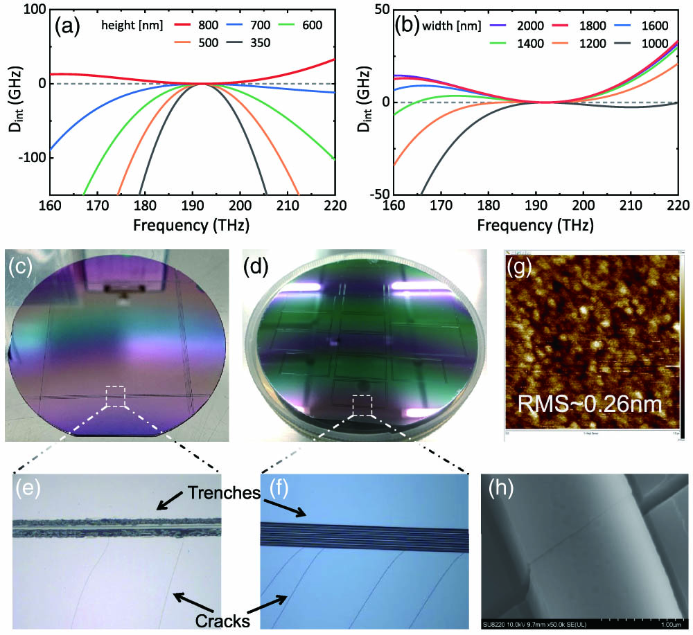
    Fig. 1. (a) Simulated dispersion curves for different heights of the Si3N4 waveguide, with the waveguide width fixed at 1.8 µm. (b) Simulated dispersion curves for different widths of the Si3N4 waveguide, with the waveguide height fixed at 800 nm. (c) Using a diamond scriber on the 4 in. wafer to draw a square area. (d) Using lithography to define the patterns of the trenches. (e), (f) The relevant partial magnifications show that the cracks are successfully blocked by the trenches. (g) The surface range of 1 µm × 1 µm is scanned by atomic force microscopy (AFM), and the corresponding root-mean-square (RMS) roughness is 0.26 nm. (h) Scanning electron microscope (SEM) image of a crack passing through the etched waveguide.
    (a) Fabrication process of the Si3N4 device. (b) SEM image of the Si3N4 microring resonator and bus waveguide. (c) SEM image of the cross-section view of the bus waveguide with photoresist, which is removed before SiO2 depositing. The microtrench is at the bottom of each sidewall of the waveguide. (d) SEM image of the cross-section view of the bus waveguide after depositing the SiO2 for protection. The Si3N4 waveguide is painted with green color.
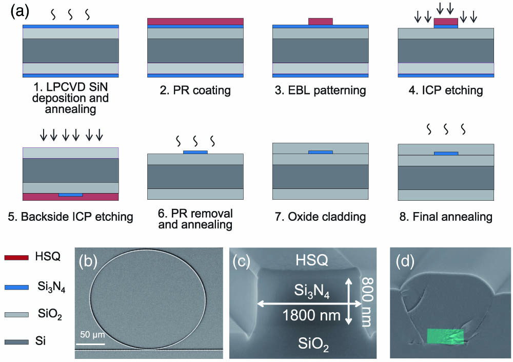
    Fig. 2. (a) Fabrication process of the Si3N4 device. (b) SEM image of the Si3N4 microring resonator and bus waveguide. (c) SEM image of the cross-section view of the bus waveguide with photoresist, which is removed before SiO2 depositing. The microtrench is at the bottom of each sidewall of the waveguide. (d) SEM image of the cross-section view of the bus waveguide after depositing the SiO2 for protection. The Si3N4 waveguide is painted with green color.
    (a) Schematic of the experimental setup. FPC, fiber polarization controller; EDFA, erbium-doped fiber amplifier; FG, function generator; OSA, optical spectrum analyzer; OSC, oscilloscope; PD, photon detector. (b) The typical transmission of fundamental TE (red curve) and TM (blue curve) modes from 1550 nm to 1630 nm. The envelope of the transmission line decreasing with the increase of wavelength is due to the power variation of the laser itself. Total insertion losses of fundamental TE modes and TM modes are about −3.6 dB and −4.5 dB, respectively.
    Fig. 3. (a) Schematic of the experimental setup. FPC, fiber polarization controller; EDFA, erbium-doped fiber amplifier; FG, function generator; OSA, optical spectrum analyzer; OSC, oscilloscope; PD, photon detector. (b) The typical transmission of fundamental TE (red curve) and TM (blue curve) modes from 1550 nm to 1630 nm. The envelope of the transmission line decreasing with the increase of wavelength is due to the power variation of the laser itself. Total insertion losses of fundamental TE modes and TM modes are about −3.6 dB and −4.5 dB, respectively.
    (a) Loaded Q of the resonances in the microring with and without the annealing process of the Si3N4 film. The diameter of the microring is 200 µm with the cross section of 1.8 µm × 800 nm. The inset shows the histogram of the linewidth of fundamental TM (blue) and TE (red) modes. (b) The typical TM optical mode with the Lorentz fitting linewidth of about 128 MHz. (c) The typical transmission spectrum of the optical mode with the linewidth of 65 MHz in another microring with the cross section of 3 µm × 800 nm.
    Fig. 4. (a) Loaded Q of the resonances in the microring with and without the annealing process of the Si3N4 film. The diameter of the microring is 200 µm with the cross section of 1.8 µm × 800  nm. The inset shows the histogram of the linewidth of fundamental TM (blue) and TE (red) modes. (b) The typical TM optical mode with the Lorentz fitting linewidth of about 128 MHz. (c) The typical transmission spectrum of the optical mode with the linewidth of 65 MHz in another microring with the cross section of 3 µm × 800 nm.
    Relationship between the output power of the primary FWM sidebands and the on-chip pump power of the microring resonator with a cross section of 1.8 µm × 800 nm and a radius of 100 µm, showing the FWM threshold of about 13.4 mW. Inset: optical spectrum with on-chip pump power of 13.9 mW.
    Fig. 5. Relationship between the output power of the primary FWM sidebands and the on-chip pump power of the microring resonator with a cross section of 1.8 µm × 800 nm and a radius of 100 µm, showing the FWM threshold of about 13.4 mW. Inset: optical spectrum with on-chip pump power of 13.9 mW.
    (a) Evolution of the intracavity power as the laser frequency is scanning across the resonance mode. (b) Schematic of auxiliary-laser-assisted thermal response control method. The optical spectra of (c) multi-soliton and (d) single soliton states with the smooth envelope fitted by the sech2 function (red curve).
    Fig. 6. (a) Evolution of the intracavity power as the laser frequency is scanning across the resonance mode. (b) Schematic of auxiliary-laser-assisted thermal response control method. The optical spectra of (c) multi-soliton and (d) single soliton states with the smooth envelope fitted by the sech2 function (red curve).
    Shuai Wan, Rui Niu, Jin-Lan Peng, Jin Li, Guang-Can Guo, Chang-Ling Zou, Chun-Hua Dong. Fabrication of the high-Q Si3N4 microresonators for soliton microcombs[J]. Chinese Optics Letters, 2022, 20(3): 032201
    Download Citation