
Shuai Wan, Rui Niu, Jin-Lan Peng, Jin Li, Guang-Can Guo, Chang-Ling Zou, Chun-Hua Dong, "Fabrication of the high-
- Chinese Optics Letters
- Vol. 20, Issue 3, 032201 (2022)
Abstract
1. Introduction
The optical frequency comb, which is a series of equidistant coherent optical lines in the frequency domain, has been greatly developed in the past two decades[
Compared with the conventional optical frequency comb generated by the mode-locked laser, the performance of the soliton microcomb has the advantages of low-power consumption, small footprint, simple structure, and integrability[
In recent years, because of the possibility to achieve ultra-low linear and nonlinear optical losses and engineer the dispersion of waveguides and microresonators precisely[
Sign up for Chinese Optics Letters TOC. Get the latest issue of Chinese Optics Letters delivered right to you!Sign up now
In this work, we adopt the traditional subtractive process to fabricate dispersion-engineered microring resonators. By introducing the crack isolation trenches and performing the annealing process to reduce the tensile stress, we successfully deposit thick stoichiometric
2. Device Fabrication
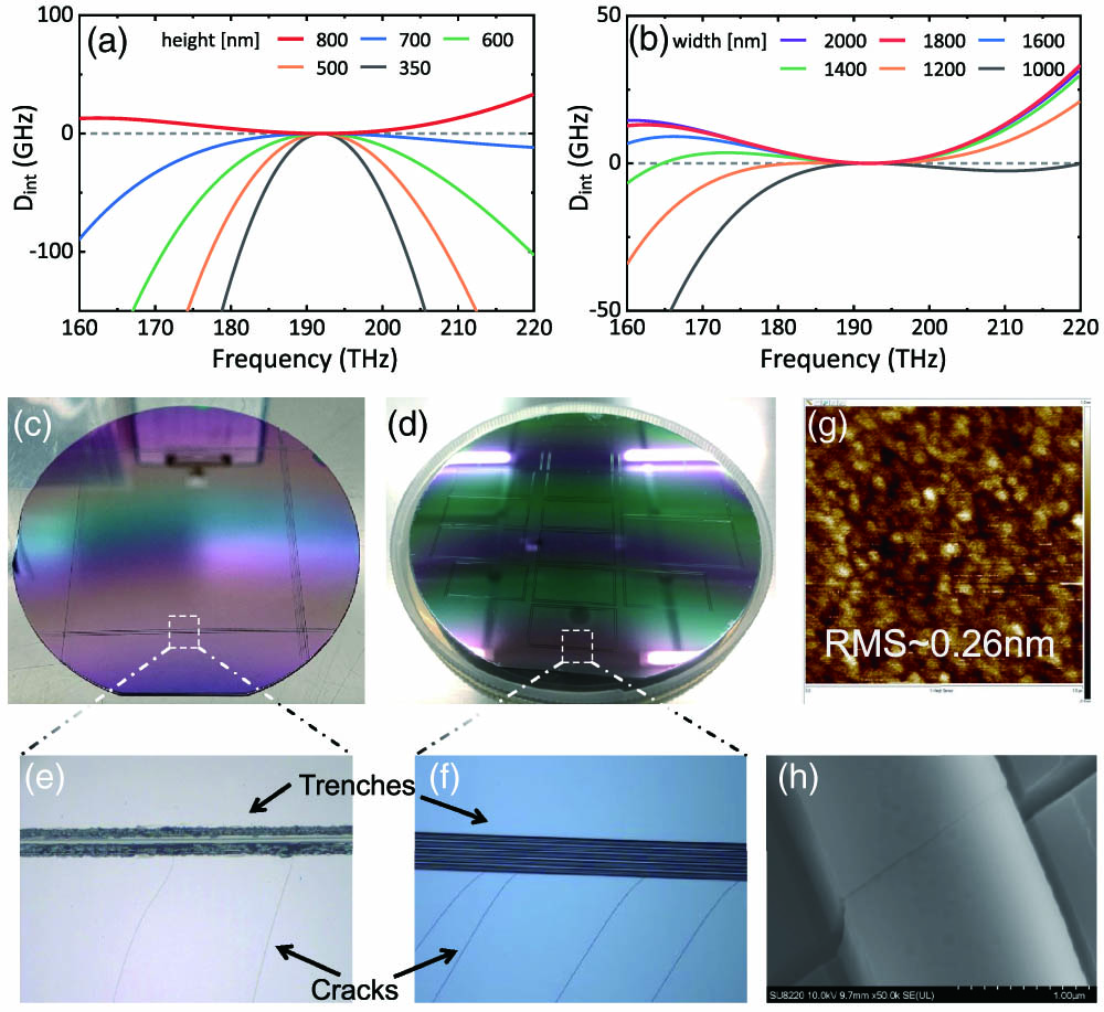
To generate the Kerr soliton in the microresonator, anomalous group velocity dispersion (GVD) is required for permitting the phase and energy matching of the nonlinear optical interactions. The material GVD of
![]()
Figure 1.(a) Simulated dispersion curves for different heights of the Si3N4 waveguide, with the waveguide width fixed at 1.8 µm. (b) Simulated dispersion curves for different widths of the Si3N4 waveguide, with the waveguide height fixed at 800 nm. (c) Using a diamond scriber on the 4 in. wafer to draw a square area. (d) Using lithography to define the patterns of the trenches. (e), (f) The relevant partial magnifications show that the cracks are successfully blocked by the trenches. (g) The surface range of 1 µm × 1 µm is scanned by atomic force microscopy (AFM), and the corresponding root-mean-square (RMS) roughness is 0.26 nm. (h) Scanning electron microscope (SEM) image of a crack passing through the etched waveguide.
From the above simulation results, for microcomb generation, the thickness of the
The subtractive fabrication flow is illustrated in Fig. 2. The device is patterned by e-beam lithography with hydrogen-silsesquioxane (HSQ) resist. Following the development of the pattern, the film is etched with a
![]()
Figure 2.(a) Fabrication process of the Si3N4 device. (b) SEM image of the Si3N4 microring resonator and bus waveguide. (c) SEM image of the cross-section view of the bus waveguide with photoresist, which is removed before SiO2 depositing. The microtrench is at the bottom of each sidewall of the waveguide. (d) SEM image of the cross-section view of the bus waveguide after depositing the SiO2 for protection. The Si3N4 waveguide is painted with green color.
3. Optical Characterization of Microring
To realize soliton microcombs, we fabricate the microring resonator with a cross section of
![]()
Figure 3.(a) Schematic of the experimental setup. FPC, fiber polarization controller; EDFA, erbium-doped fiber amplifier; FG, function generator; OSA, optical spectrum analyzer; OSC, oscilloscope; PD, photon detector. (b) The typical transmission of fundamental TE (red curve) and TM (blue curve) modes from 1550 nm to 1630 nm. The envelope of the transmission line decreasing with the increase of wavelength is due to the power variation of the laser itself. Total insertion losses of fundamental TE modes and TM modes are about −3.6 dB and −4.5 dB, respectively.
The loaded Q of all TM and TE resonances within the measurement spectrum (blue and red cross) are extracted and shown in Fig. 4(a), and the loaded Q of the microring resonator fabricated from the
![]()
Figure 4.(a) Loaded Q of the resonances in the microring with and without the annealing process of the Si3N4 film. The diameter of the microring is 200 µm with the cross section of 1.8 µm × 800 nm. The inset shows the histogram of the linewidth of fundamental TM (blue) and TE (red) modes. (b) The typical TM optical mode with the Lorentz fitting linewidth of about 128 MHz. (c) The typical transmission spectrum of the optical mode with the linewidth of 65 MHz in another microring with the cross section of 3 µm × 800 nm.
To explore the narrowest linewidth available with our current processing technology, we fabricate the microring resonator with the same radius and height, but with a larger ring width of 3 µm. Because of the relatively large ring width, scattering loss from etched sidewalls is reduced. As shown in Fig. 4(c), the linewidth of the optical mode at 1552.6 nm is about 65 MHz, corresponding to a loaded
FWM is the basis of frequency comb generation, and the threshold is inversely proportional to squared Q. Therefore, the next step is to characterize the FWM threshold of our device, which has a cross section of
![]()
Figure 5.Relationship between the output power of the primary FWM sidebands and the on-chip pump power of the microring resonator with a cross section of 1.8 µm × 800 nm and a radius of 100 µm, showing the FWM threshold of about 13.4 mW. Inset: optical spectrum with on-chip pump power of 13.9 mW.
4. Soliton Microcombs
Further increasing the pump power and tuning the frequency of the pump laser, a series of frequency comb states and final soliton state can be generated from our device. To investigate the evolution of the comb states, the pump laser amplified by the erbium-doped fiber amplifier (EDFA) with an input power
![]()
Figure 6.(a) Evolution of the intracavity power as the laser frequency is scanning across the resonance mode. (b) Schematic of auxiliary-laser-assisted thermal response control method. The optical spectra of (c) multi-soliton and (d) single soliton states with the smooth envelope fitted by the sech2 function (red curve).
To compensate the influence of the thermal effect in the high Q microring, as shown in Fig. 3(a), another auxiliary laser (red) is coupled to another optical mode in the opposite direction of pump laser[
5. Conclusion
In conclusion, we have presented the fabrication process of crack-free stoichiometric LPCVD
References
[1] T. J. Kippenberg, R. Holzwarth, S. A. Diddams. Microresonator-based optical frequency combs. Science, 332, 555(2011).
[2] T. J. Kippenberg, A. L. Gaeta, M. Lipson, M. L. Gorodetsky. Dissipative Kerr solitons in optical microresonators. Science, 361, eaan8083(2018).
[3] S. A. Diddams, K. Vahala, T. Udem. Optical frequency combs: coherently uniting the electromagnetic spectrum. Science, 369, eaay3676(2020).
[4] S. A. Diddams, D. J. Jones, J. Ye, S. T. Cundiff, J. L. Hall, J. K. Ranka, R. S. Windeler, R. Holzwarth, T. Udem, T. W. Hänsch. Direct link between microwave and optical frequencies with a 300 THz femtosecond laser comb. Phys. Rev. Lett., 84, 5102(2000).
[5] D. J. Jones, S. A. Diddams, J. K. Ranka, A. Stentz, R. S. Windeler, J. L. Hall, S. T. Cundiff. Carrier-envelope phase control of femtosecond mode-locked lasers and direct optical frequency synthesis. Science, 288, 635(2000).
[6] T. Udem, R. Holzwarth, T. W. Hänsch. Optical frequency metrology. Nature, 416, 233(2002).
[7] P. Del’Haye, A. Schliesser, O. Arcizet, T. Wilken, R. Holzwarth, T. J. Kippenberg. Optical frequency comb generation from a monolithic microresonator. Nature, 450, 1214(2007).
[8] T. Herr, K. Hartinger, J. Riemensberger, C. Wang, E. Gavartin, R. Holzwarth, M. Gorodetsky, T. Kippenberg. Universal formation dynamics and noise of Kerr-frequency combs in microresonators. Nat. Photonics, 6, 480(2012).
[9] T. Herr, V. Brasch, J. D. Jost, C. Y. Wang, N. M. Kondratiev, M. L. Gorodetsky, T. J. Kippenberg. Temporal solitons in optical microresonators. Nat. Photonics, 8, 145(2014).
[10] H. Weng, J. Liu, A. Afridi, J. Li, J. Dai, X. Ma, Y. Zhang, Q. Lu, J. Donegan, W. Guo. Directly accessing octave-spanning dissipative Kerr soliton frequency combs in an AlN microresonator. Photonics Res., 9, 1351(2021).
[11] X. Wang, P. Xie, W. Wang, Y. Wang, Z. Lu, L. Wang, S. Chu, B. Little, W. Zhao, W. Zhang. Program-controlled single soliton microcomb source. Photonics Res., 9, 66(2021).
[12] Z. Lu, H.-J. Chen, W. Wang, L. Yao, Y. Wang, Y. Yu, B. E. Little, S. T. Chu, Q. Gong, W. Zhao, X. Yi, Y.-F. Xiao, W. Zhang. Synthesized soliton crystals. Nat. Commun., 12, 3179(2021).
[13] W. Wang, L. Wang, W. Zhang. Advances in soliton microcomb generation. Adv. Photonics, 2, 034001(2020).
[14] B. Shen, L. Chang, J. Liu, H. Wang, Q.-F. Yang, C. Xiang, R. N. Wang, J. He, T. Liu, W. Xie, J. Guo, D. Kinghorn, L. Wu, Q.-X. Ji, T. J. Kippenberg, K. Vahala, J. E. Bowers. Integrated turnkey soliton microcombs. Nature, 582, 365(2020).
[15] H.-J. Chen, Q.-X. Ji, H. Wang, Q.-F. Yang, Q.-T. Cao, Q. Gong, X. Yi, Y.-F. Xiao. Chaos-assisted two-octave-spanning microcombs. Nat. Commun., 11, 2336(2020).
[16] F. Shu, P. Zhang, Y. Qian, Z. Wang, S. Wan, C. Zou, G. Guo, C. Dong. A mechanically tuned Kerr comb in a dispersion-engineered silica microbubble resonator. Sci. China: Phys. Mech. Astron., 63, 254211(2020).
[17] Q. Zhang, B. Liu, Q. Wen, J. Qin, Y. Geng, Q. Zhou, G. Deng, K. Qiu, H. Zhou. Low-noise amplification of dissipative Kerr soliton microcomb lines via optical injection locking lasers. Chin. Opt. Lett., 19, 121401(2021).
[18] D. T. Spencer, T. Drake, T. C. Briles, J. Stone, L. C. Sinclair, C. Fredrick, Q. Li, D. Westly, B. R. Ilic, A. Bluestone, N. Volet, T. Komljenovic, L. Chang, S. H. Lee, D. Y. Oh, M.-G. Suh, K. Y. Yang, M. H. P. Pfeiffer, T. J. Kippenberg, E. Norberg, L. Theogarajan, K. Vahala, N. R. Newbury, K. Srinivasan, J. E. Bowers, S. A. Diddams, S. B. Papp. An optical-frequency synthesizer using integrated photonics. Nature, 557, 81(2018).
[19] Z. L. Newman, V. Maurice, T. Drake, J. R. Stone, T. C. Briles, D. T. Spencer, C. Fredrick, Q. Li, D. Westly, B. R. Ilic, B. Shen, M.-G. Suh, K. Y. Yang, C. Johnson, D. M. S. Johnson, L. Hollberg, K. J. Vahala, K. Srinivasan, S. A. Diddams, J. Kitching, S. B. Papp, M. T. Hummon. Architecture for the photonic integration of an optical atomic clock. Optica, 6, 680(2019).
[20] M.-G. Suh, K. J. Vahala. Soliton microcomb range measurement. Science, 359, 884(2018).
[21] P. Trocha, M. Karpov, D. Ganin, M. H. P. Pfeiffer, A. Kordts, S. Wolf, J. Krockenberger, P. Marin-Palomo, C. Weimann, S. Randel, W. Freude, T. J. Kippenberg, C. Koos. Ultrafast optical ranging using microresonator soliton frequency combs. Science, 359, 887(2018).
[22] J. Riemensberger, A. Lukashchuk, M. Karpov, W. Weng, E. Lucas, J. Liu, T. J. Kippenberg. Massively parallel coherent laser ranging using a soliton microcomb. Nature, 581, 164(2020).
[23] J. Wang, Z. Lu, W. Wang, F. Zhang, J. Chen, Y. Wang, J. Zheng, S. Chu, W. Zhao, B. Little, X. Qu, W. Zhang. Long-distance ranging with high precision using a soliton microcomb. Photonics Res., 8, 1964(2020).
[24] W. Liang, D. Eliyahu, V. S. Ilchenko, A. A. Savchenkov, A. B. Matsko, D. Seidel, L. Maleki. High spectral purity Kerr frequency comb radio frequency photonic oscillator. Nat. Commun., 6, 7957(2015).
[25] W. Weng, E. Lucas, G. Lihachev, V. E. Lobanov, H. Guo, M. L. Gorodetsky, T. J. Kippenberg. Spectral purification of microwave signals with disciplined dissipative Kerr solitons. Phys. Rev. Lett., 122, 013902(2019).
[26] E. Lucas, P. Brochard, R. Bouchand, S. Schilt, T. Südmeyer, T. J. Kippenberg. Ultralow-noise photonic microwave synthesis using a soliton microcomb-based transfer oscillator. Nat. Commun., 11, 374(2020).
[27] J. Liu, E. Lucas, A. S. Raja, J. He, J. Riemensberger, R. N. Wang, M. Karpov, H. Guo, R. Bouchand, T. J. Kippenberg. Photonic microwave generation in the X- and K-band using integrated soliton microcombs. Nat. Photonics, 14, 486(2020).
[28] P. Marin-Palomo, J. N. Kemal, M. Karpov, A. Kordts, J. Pfeifle, M. H. P. Pfeiffer, P. Trocha, S. Wolf, V. Brasch, M. H. Anderson, R. Rosenberger, K. Vijayan, W. Freude, T. J. Kippenberg, C. Koos. Microresonator-based solitons for massively parallel coherent optical communications. Nature, 546, 274(2017).
[29] B. Corcoran, M. Tan, X. Xu, A. Boes, J. Wu, T. G. Nguyen, S. T. Chu, B. E. Little, R. Morandotti, A. Mitchell, D. J. Moss. Ultra-dense optical data transmission over standard fibre with a single chip source. Nat. Commun., 11, 2568(2020).
[30] F.-X. Wang, W. Wang, R. Niu, X. Wang, C.-L. Zou, C.-H. Dong, B. E. Little, S. T. Chu, H. Liu, P. Hao, S. Liu, S. Wang, Z.-Q. Yin, D.-Y. He, W. Zhang, W. Zhao, Z.-F. Han, G.-C. Guo, W. Chen. Quantum key distribution with on-chip dissipative Kerr soliton. Laser Photonics Rev., 14, 1900190(2020).
[31] M.-G. Suh, Q.-F. Yang, K. Y. Yang, X. Yi, K. J. Vahala. Microresonator soliton dual-comb spectroscopy. Science, 354, 600(2016).
[32] A. Dutt, C. Joshi, X. Ji, J. Cardenas, Y. Okawachi, K. Luke, A. L. Gaeta, M. Lipson. On-chip dual-comb source for spectroscopy. Sci. Adv., 4, e1701858(2018).
[33] M. Yu, Y. Okawachi, A. G. Griffith, N. Picqué, M. Lipson, A. L. Gaeta. Silicon-chip-based mid-infrared dual-comb spectroscopy. Nat. Commun., 9, 1869(2018).
[34] Q.-F. Yang, B. Shen, H. Wang, M. Tran, Z. Zhang, K. Y. Yang, L. Wu, C. Bao, J. Bowers, A. Yariv, K. Vahala. Vernier spectrometer using counterpropagating soliton microcombs. Science, 363, 965(2019).
[35] X. Ji, X. Yao, A. Klenner, Y. Gan, A. L. Gaeta, C. P. Hendon, M. Lipson. Chip-based frequency comb sources for optical coherence tomography. Opt. Express, 27, 19896(2019).
[36] P. J. Marchand, J. Connor Skehan, J. Riemensberger, J.-J. Ho, M. H. P. Pfeiffer, J. Liu, C. Hauger, T. Lasser, T. J. Kippenberg. Soliton microcomb based spectral domain optical coherence tomography. Nat. Commun., 12, 427(2021).
[37] D. J. Moss, R. Morandotti, A. L. Gaeta, M. Lipson. New CMOS-compatible platforms based on silicon nitride and Hydex for nonlinear optics. Nat. Photonics, 7, 597(2013).
[38] S. Wan, R. Niu, Z.-Y. Wang, J.-L. Peng, M. Li, J. Li, G.-C. Guo, C.-L. Zou, C.-H. Dong. Frequency stabilization and tuning of breathing soliton in Si3N4 microresonators. Photonics Res., 8, 1342(2020).
[39] A. Rahim, E. Ryckeboer, A. Z. Subramanian, S. Clemmen, B. Kuyken, A. Dhakal, A. Raza, A. Hermans, M. Muneeb, S. Dhoore, Y. Li, U. Dave, P. Bienstman, N. Le Thomas, G. Roelkens, D. Van Thourhout, P. Helin, S. Severi, X. Rottenberg, R. Baets. Expanding the silicon photonics portfolio with silicon nitride photonic integrated circuits. J. Lightw. Technol., 35, 639(2017).
[40] K. M. Latt, H. Park, H. Seng, T. Osipowicz, Y. Lee, S. Li. Effect of the silicon nitride passivation layer on the Cu/Ta/SiO2/Si multi-layer structure. Mater. Sci. Eng. B, 90, 25(2002).
[41] M. W. Puckett, K. Liu, N. Chauhan, Q. Zhao, N. Jin, H. Cheng, J. Wu, R. O. Behunin, J. Wu, P. T. Rakich, K. D. Nelson, D. J. Blumenthal. 422 million intrinsic quality factor planar integrated all-waveguide resonator with sub-MHz linewidth. Nat. Commun., 12, 934(2021).
[42] M. H. P. Pfeiffer, A. Kordts, V. Brasch, M. Zervas, M. Geiselmann, J. D. Jost, T. J. Kippenberg. Photonic damascene process for integrated high-Q microresonator based nonlinear photonics. Optica, 3, 20(2016).
[43] M. H. P. Pfeiffer, J. Liu, A. S. Raja, T. Morais, B. Ghadiani, T. J. Kippenberg. Ultra-smooth silicon nitride waveguides based on the damascene reflow process: fabrication and loss origins. Optica, 5, 884(2018).
[44] M. H. P. Pfeiffer, C. Herkommer, J. Liu, T. Morais, M. Zervas, M. Geiselmann, T. J. Kippenberg. Photonic Damascene process for low-loss, high-confinement silicon nitride waveguides. IEEE J. Sel. Top. Quantum Electron., 24, 6101411(2018).
[45] X. Zhang, G. Lin, T. Sun, Q. Song, G. Xiao, H. Luo. Dispersion engineering and measurement in crystalline microresonators using a fiber ring etalon. Photonics Res., 9, 2222(2021).
[46] K. Luke, A. Dutt, C. B. Poitras, M. Lipson. Overcoming Si3N4 film stress limitations for high quality factor ring resonators. Opt. Express, 21, 22829(2013).
[47] Y. Xuan, Y. Liu, L. T. Varghese, A. J. Metcalf, X. Xue, P.-H. Wang, K. Han, J. A. Jaramillo-Villegas, A. Al Noman, C. Wang, S. Kim, M. Teng, Y. J. Lee, B. Niu, L. Fan, J. Wang, D. E. Leaird, A. M. Weiner, M. Qi. High-Q silicon nitride microresonators exhibiting low-power frequency comb initiation. Optica, 3, 1171(2016).
[48] K. H. Nam, I. H. Park, S. H. Ko. Patterning by controlled cracking. Nature, 485, 221(2012).
[49] B. Kim, J. Bae, B. T. Lee. Microtrench depth and width of SiON plasma etching. Vacuum, 81, 338(2006).
[50] M. H. P. Pfeiffer, J. Liu, M. Geiselmann, T. J. Kippenberg. Coupling ideality of integrated planar high-Q microresonators. Phys. Rev. Appl., 7, 024026(2017).
[51] H. Zhou, Y. Geng, W. Cui, S.-W. Huang, Q. Zhou, K. Qiu, C. W. Wong. Soliton bursts and deterministic dissipative Kerr soliton generation in auxiliary-assisted microcavities. Light Sci. Appl., 8, 50(2019).
[52] X. Liu, X.-S. Yan, X. Zhang, Y. Liu, H. Li, Y. Chen, X. Chen. Tunable single-mode laser on thin film lithium niobate. Opt. Lett., 46, 5505(2021).
[53] Z. Lu, W. Wang, W. Zhang, S. T. Chu, B. E. Little, M. Liu, L. Wang, C.-L. Zou, C.-H. Dong, B. Zhao, W. Zhao. Deterministic generation and switching of dissipative Kerr soliton in a thermally controlled micro-resonator. AIP Adv., 9, 25314(2019).
[54] X. Yi, Q.-F. Yang, X. Zhang, K. Y. Yang, X. Li, K. Vahala. Single-mode dispersive waves and soliton microcomb dynamics. Nat. Commun., 8, 14869(2017).
[55] C. Bao, Y. Xuan, D. E. Leaird, S. Wabnitz, M. Qi, A. M. Weiner. Spatial mode-interaction induced single soliton generation in microresonators. Optica, 4, 1011(2017).
[56] Z. Wang, C. Wu, Z. Fang, M. Wang, J. Lin, R. Wu, J. Zhang, J. Yu, M. Wu, W. Chu, T. Lu, G. Chen, Y. Cheng. High-quality-factor optical microresonators fabricated on lithium niobate thin film with an electro-optical tuning range spanning over one free spectral range. Chin. Opt. Lett., 19, 060002(2021).
[57] J. Lin, F. Bo, Y. Cheng, J. Xu. Advances in on-chip photonic devices based on lithium niobate on insulator. Photonics Res., 8, 1910(2020).


Set citation alerts for the article
Please enter your email address

© Copyright 2018-2021 | Chinese Laser Press. All Rights Reserved 沪ICP备15018463号-20