
Qiaoli Liu, Yajie Feng, Huijun Tian, Xiaoying He, Anqi Hu, Xia Guo. Fabrication of flexible AlGaInP LED[J]. Journal of Semiconductors, 2020, 41(3): 032302
- Journal of Semiconductors
- Vol. 41, Issue 3, 032302 (2020)
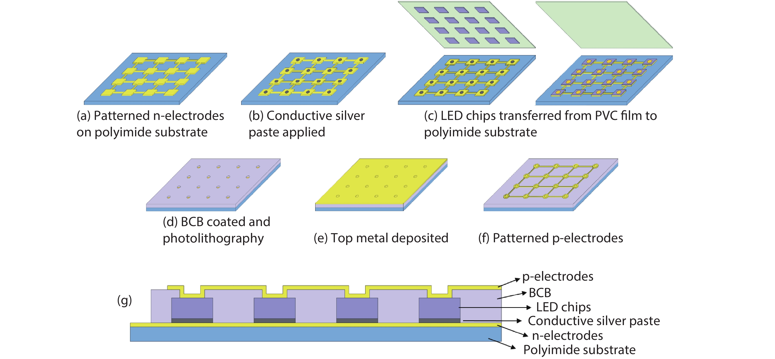
Fig. 1. (Color online) Illustration of fabrication process of flexible LEDs. (a) After Ti/Au layer deposition and photolithography, the bottom n-electrodes are patterned on the polyimide substrate. (b) Application of conductive silver paste. (c) Transfer of LED chips from PVC film to polyimide substrate. (d) BCB coating and then photolithography to expose the top electrodes of LEDs. (e) Top metal layer deposition. (f) Patterned top p-electrodes after photolithography. (g) Schematic cross section of flexible LEDs.
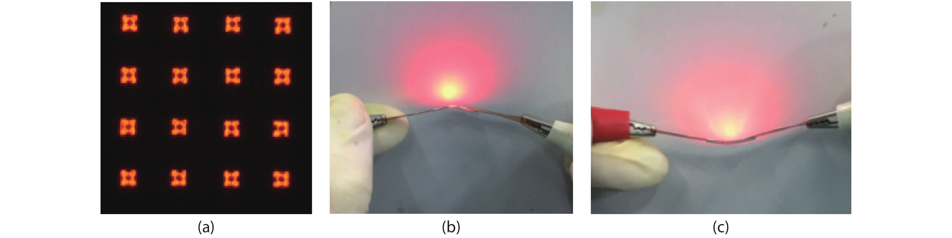
Fig. 2. (Color online) (a) Metallurgical microscope image of the transferred LED arrays under the current injection of 1 mA. (b) and (c) Side-view images of concave and convex bent LED arrays, respectively.
Fig. 3. (Color online) (a) Comparison of forward I–V characteristics of transferred LED array before and after bending with the curvature of 5, 8, and 11 mm, respectively. The voltage drop is 2 V under the current injection of 20 mA. (b) EL spectra comparison of the transferred LED under the current injection of 5 mA before and after bending. The red-shift of peak wavelength is due to heat.

Set citation alerts for the article
Please enter your email address
© Copyright 2018-2021 | Chinese Laser Press. All Rights Reserved 沪ICP备15018463号-20