
Qiaoli Liu, Yajie Feng, Huijun Tian, Xiaoying He, Anqi Hu, Xia Guo. Fabrication of flexible AlGaInP LED[J]. Journal of Semiconductors, 2020, 41(3): 032302
- Journal of Semiconductors
- Vol. 41, Issue 3, 032302 (2020)
Abstract
1. Introduction
High-efficiency semiconductor light-emitting diodes (LEDs) are now widely used in the field of display, lighting, etc. to replace the traditional incandescent or fluorescent lamp for energy saving[
Organic light-emitting diodes (OLED) are naturally flexible[
The wavelength of quaternary material AlGaInP LED ranges from 560 to 650 nm at room temperature, which is widely applied in the fields of display, lighting, etc. For the flexible type, Rogers’ group developed a type of waterproof AlGaInP LED on a flexible substrate for biomedical and robotics applications[
In the large-scale LED manufacture process, LED chips will be put on a piece of blue PVC film after dicing. The space between the adjacent chips can be controlled by uniform pulling force applied on the heated PVC film for both AlGaInP and GaN LEDs. In this paper, a 4 × 4 flexible AlGaInP LED array is fabricated by transferring the LED chips from the blue PVC films to flexible polyimide substrate directly. Such a fabrication process is much easier, mature and high-yield compared with the previously reported methods.
2. Experiment
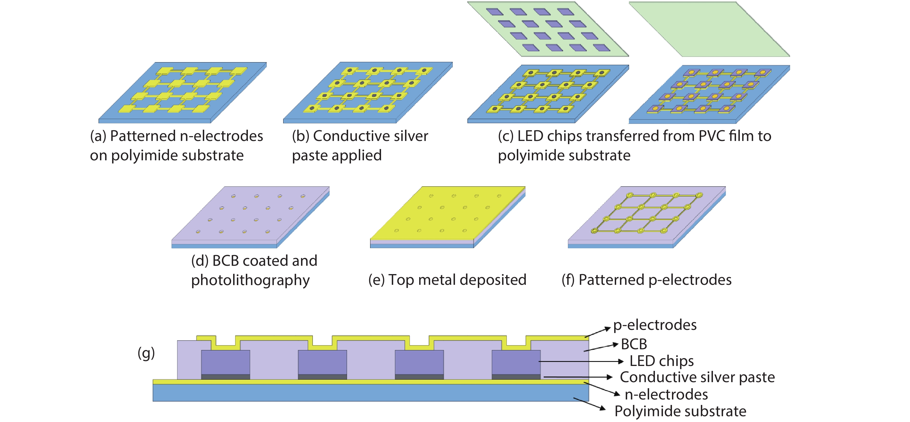
Figs. 1(a)–1(f) illustrate the fabrication process of the flexible AlGaInP LEDs. Firstly, a Ti/Au (15 nm/150 nm) layer is deposited on the polyimide substrate (DuPont, Kapton 500HN), which has excellent physical, chemical and electrical performance. After photolithography, the bottom n-electrodes are patterned on the polyimide substrate. The square bottom n-electrodes are connected by straight metal lines with a width of 200 μm and length of 430 μm. After conductive silver paste is applied on the center of the Ti/Au electrodes, the center of the LED chips stuck on the PVC film are aligned to the center of the bottom n-electrodes on the polyimide film with pressure under the microscope. Then it is put into an oven at 150 °C for 1 h for curing. The PVC film can be peeled easily from the chips because the viscosity of PVC film decreases a lot due to the high temperature. The LED chips finish by being transferred to the polyimide substrate and electrical connection. Then BCB (benzocyclobutene) is coated on the top for electronic isolation between the p- and n-electrodes. After heating for around 1 h with gradient rising temperature, the liquid BCB becomes transparent, which indicates little absorption. After exposing the top electrode of LEDs by photolithography, Ti/Au (15 nm/150 nm) layers are deposited on the BCB layer. Finally, the p-electrodes are connected by metal lines after photolithography and wet etching. The 4 × 4 array is formed, and the schematic cross section is illustrated in Fig. 1(g).
![]()
Figure 1.(Color online) Illustration of fabrication process of flexible LEDs. (a) After Ti/Au layer deposition and photolithography, the bottom n-electrodes are patterned on the polyimide substrate. (b) Application of conductive silver paste. (c) Transfer of LED chips from PVC film to polyimide substrate. (d) BCB coating and then photolithography to expose the top electrodes of LEDs. (e) Top metal layer deposition. (f) Patterned top p-electrodes after photolithography. (g) Schematic cross section of flexible LEDs.
3. Results and discussion
Fig. 2(a) shows the emission image of 4 × 4 arrays under the current injection of 1 mA taken by the metallurgical microscope. All the LED chips are illuminating uniformly. Figs. 2(b) and 2(c) demonstrate the side-view images of the LED array with concave and convex bending. The emission intensity is constant and is also not influenced by the bending process.
![]()
Figure 2.(Color online) (a) Metallurgical microscope image of the transferred LED arrays under the current injection of 1 mA. (b) and (c) Side-view images of concave and convex bent LED arrays, respectively.
Fig. 3(a) compares the forward current–voltage (I–V) curves of transferred LEDs when it is flat (before bending) and bent with curvature of 5, 8, and 11 mm, respectively. At 20 mA, the voltage drop is around 2 V. And the ideality factor is 2.10, 2.12, 2.09, and 2.11, respectively, with the corresponding series resistance of 7.3, 6.7, 7.1, and 7.1 Ω. However, it can be seen that the I–V curves can almost coincide together, which indicates the bending process has little effect on the electrical performance due to the better ductibility of Au. Fig. 3(b) compares the electroluminescence (EL) spectra of transferred LEDs before and after bending, measured by integrating sphere from Ocean optics. The bending curvature is 11 mm. The peak of the EL spectra is 635.7 and 637.6 nm, respectively. The red-shift of the EL spectra is due to the heat during the continuous measurement. Bending only occurs in the flexible metal electrodes, which will not affect the characteristics of the LED chips. However, in the case of bending LED chips, it will introduce mechanical damage to the AlGaInP film, which will damage its performance. In the case of GaN-based LEDs, bending affects the internal quantum efficiency and emission wavelength, which adds up additional functionality of flexible LEDs[
![]()
Figure 3.(Color online) (a) Comparison of forward
4. Conclusion
In this paper, we proposed a fabrication process of flexible LED array by utilizing a mature LED manufacture technique. The key point is transferring the LED chips on the blue PVC film to the polyimide film directly. The electrical and optical performances keep well after transfer process even in the bending state. Such method keeps good yield and good optoelectronic performance at the same time.
Acknowledgments
This work was supported by the National Key R&D Program of China (2016YFB0400603).
References
[1] P M Pattison, M Hansen, J Y Tsao. LED lighting efficacy: status and directions. Compt Rend Phys, 19, 134(2018).
[2] G B Nair, S J Dhoble. A perspective perception on the applications of light-emitting diodes. Luminescence, 30, 1167(2015).
[3] H Hirayama, S Fujikawa, N Kamata. Recent progress in AlGaN-based deep-UV LEDs. Electron Commun Jpn, 98, 1(2015).
[4] B Guilhabert, D Massoubre, E Richardson et al. Sub-micron lithography using InGaN micro-LEDs: mask-free fabrication of LED arrays. IEEE Photonic Tech Lett, 24, 2221(2012).
[5] S Y Lee, K I Park, C Huh et al. Water-resistant flexible GaN LED on a liquid crystal polymer substrate for implantable biomedical applications. Nano Energy, 1, 145(2012).
[6] M K Choi, J Yang, K Kang et al. Wearable red-green-blue quantum dot light-emitting diode array using high-resolution intaglio transfer printing. Nat Commun, 6, 7149(2015).
[7] J Kim, J Lee, D Son et al. Deformable devices with integrated functional nanomaterials for wearable electronics. Nano Converg, 3, 4(2016).
[8] Z Zhang, J Du, D Zhang et al. Rosin-enabled ultraclean and damage-free transfer of graphene for large-area flexible organic light-emitting diodes. Nat Commun, 8, 14560(2017).
[9] S Kim, H J Kwon, S Lee et al. Low-power flexible organic light-emitting diode display device. Adv Mater, 23, 3511(2011).
[10] T Sekitani, H Nakajima, H Maeda et al. Stretchable active-matrix organic light-emitting diode display using printable elastic conductors. Nat Mater, 8, 494(2009).
[11] B Geffroy, P Le Roy, C Prat. Organic light-emitting diode (OLED) technology: materials, devices and display technologies. Polym Int, 55, 572(2006).
[12] Z Sun, Z Liu, J Li et al. Infrared photodetectors based on CVD-grown graphene and PbS quantum dots with ultrahigh responsivity. Adv Mater, 24, 5878(2012).
[13] L Tao, Z Chen, X Li et al. Hybrid graphene tunneling photoconductor with interface engineering towards fast photoresponse and high responsivity. npj 2D Mater Appl, 1, 19(2017).
[14] Y L Sun, D Xie, M Sun et al. Hybrid graphene/cadmium-free ZnSe/ZnS quantum dots phototransistors for UV detection. Sci Rep, 8, 5107(2018).
[15] T Sun, Y Wang, W Yu et al. Flexible broadband graphene photodetectors enhanced by plasmonic Cu3–
[16] R H Kim, D H Kim, J Xiao et al. Waterproof AlInGaP optoelectronics on stretchable substrates with applications in biomedicine and robotics. Nat Mater, 9, 929(2010).
[17] D Gao, W Wang, Z Liang et al. Design of micro, flexible light-emitting diode arrays and fabrication of flexible electrodes. J Phys D, 49, 405108(2016).
[18] S Shervin, S H Kim, M Asadirad et al. Bendable III–N visible light-emitting diodes beyond mechanical flexibility: Theoretical study on quantum efficiency improvement and color tunability by external strain. ACS Photon, 3, 486(2016).
[19] C F Lin, C L Su, H M Wu et al. Bendable InGaN light-emitting nanomembranes with tunable emission wavelength. ACS Appl Mater Inter, 10, 37725(2018).


Set citation alerts for the article
Please enter your email address

© Copyright 2018-2021 | Chinese Laser Press. All Rights Reserved 沪ICP备15018463号-20