
Huixin Qi, Zhuochen Du, Xiaoyong Hu, Jiayu Yang, Saisai Chu, Qihuang Gong. High performance integrated photonic circuit based on inverse design method[J]. Opto-Electronic Advances, 2022, 5(10): 210061
- Opto-Electronic Advances
- Vol. 5, Issue 10, 210061 (2022)
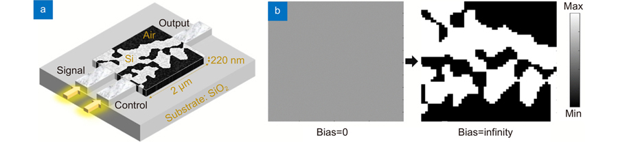
Fig. 1. Design optimization process of the all-optical switch. (a ) General configuration of the all-optical switch. (b ) The initialization and discrete optimization permittivity distribution in the x-y two-dimensional cross-section, where bias=0 and bias=infinity.
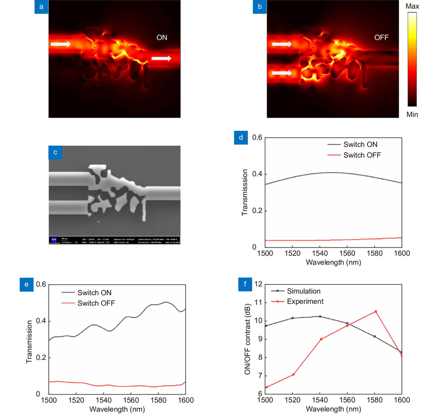
Fig. 2. Characterization of the all-optical switch. (a ) The “ON” state of normalized intensity distribution in the x-y plane from theoretical calculation. (b ) The “OFF” state of normalized intensity distribution in the x-y plane from theoretical calculation. (c ) Scanning electron microscopy (SEM) image of the all-optical switch. The size of the optimized area was 2 μm×2 μm. (d ) Simulation results of the transmission of all-optical switch. (e ) Experiment results of the normalized transmission of all-optical switch. (f ) The simulation and experiment results of the all-optical switch ON/OFF contrast.
Fig. 3. Characterization of the all-optical switch. (a ) The “OFF” state of normalized intensity distribution in the x-y plane from theoretical calculation at t=0 fs. (b–d ) The “ON” state of normalized intensity distribution in the x-y plane from theoretical calculation at t=40 fs, 80 fs and 100 fs, respectively. (e ) Transmission of the output of the all-optical switch under different delay time at 1500 nm-1600 nm. (f ) Transmission of the output of the all-optical switch under different delay time at 1500 nm.
Fig. 4. Design optimization process of all-optical XOR logic gate. (a ) General configuration of the all-optical XOR logic gate. (b ) The initialization and discrete optimization permittivity distribution in the x-y two-dimensional cross-section, where bias=0 and bias=infinity.
Fig. 5. Characterization of the all-optical XOR logic gate. (a ) The “01” input of normalized intensity distribution in the x-y plane from theoretical calculation. (b ) The “10” input of normalized intensity distribution in the x-y plane from theoretical calculation. (c ) The “11” input of normalized intensity distribution in the x-y plane from theoretical calculation. (d ) Scanning electron microscopy (SEM)image of the XOR logic gate. The size of the optimized area was 2 μm×2 μm. (e ) Simulation results of the transmission of all-optical switch. (f ) Experiment results of the normalized transmission of all-optical XOR logic gate.
Fig. 6. Characterization of the all-optical integrated circuit. (a ) General configuration of the all-optical integrated circuit. (b ) The “11” input (“ON” and ”ON” states) of normalized intensity distribution in the x-y plane from theoretical calculation. (c ) The “10” input (“ON” and ”OFF” states) of normalized intensity distribution in the x-y plane from theoretical calculation. (d ) The “01” input (“OFF” and ”ON” states) of normalized intensity distribution in the x-y plane from theoretical calculation. (e ) The “00” input (“OFF” and ”OFF” states) of normalized intensity distribution in the x-y plane from theoretical calculation.
Fig. 7. Characterization of the all-optical integrated circuit. (a ) Scanning electron microscopy (SEM) image of the all-optical integrated circuit. The size of the optimized area was 2.5 μm×7 μm. (b ) Simulation results of the transmission of the all-optical integrated circuit. (c ) Experiment results of the normalized transmission of the all-optical integrated circuit.
| ||||||||||||||||||||||||||||||
Table 0. The “ON” and “OFF” state of the all-optical switch and the true value of the XOR logic gate in the integrated photonics circuit.
|
Table 0. The two-digit state of logic signal 1 and logic signal 2 of the all-optical integrated photonic circuit and the identifying result.


Set citation alerts for the article
Please enter your email address

© Copyright 2018-2021 | Chinese Laser Press. All Rights Reserved 沪ICP备15018463号-20