The basic indexes of all-optical integrated photonic circuits include high-density integration, ultrafast response and ultra-low energy consumption. Traditional methods mainly adopt conventional micro/nano-structures. The overall size of the circuit is large, usually reaches hundreds of microns. Besides, it is difficult to balance the ultrafast response and ultra-low energy consumption problem, and the crosstalk between two traditional devices is difficult to overcome. Here, we propose and experimentally demonstrate an approach based on inverse design method to realize a high-density, ultrafast and ultra-low energy consumption integrated photonic circuit with two all-optical switches controlling the input states of an all-optical XOR logic gate. The feature size of the whole circuit is only 2.5 μm × 7 μm, and that of a single device is 2 μm × 2 μm. The distance between two adjacent devices is as small as 1.5 μm, within wavelength magnitude scale. Theoretical response time of the circuit is 150 fs, and the threshold energy is within 10 fJ/bit. We have also considered the crosstalk problem. The circuit also realizes a function of identifying two-digit logic signal results. Our work provides a new idea for the design of ultrafast, ultra-low energy consumption all-optical devices and the implementation of high-density photonic integrated circuits.The basic indexes of all-optical integrated photonic circuits include high-density integration, ultrafast response and ultra-low energy consumption. Traditional methods mainly adopt conventional micro/nano-structures. The overall size of the circuit is large, usually reaches hundreds of microns. Besides, it is difficult to balance the ultrafast response and ultra-low energy consumption problem, and the crosstalk between two traditional devices is difficult to overcome. Here, we propose and experimentally demonstrate an approach based on inverse design method to realize a high-density, ultrafast and ultra-low energy consumption integrated photonic circuit with two all-optical switches controlling the input states of an all-optical XOR logic gate. The feature size of the whole circuit is only 2.5 μm × 7 μm, and that of a single device is 2 μm × 2 μm. The distance between two adjacent devices is as small as 1.5 μm, within wavelength magnitude scale. Theoretical response time of the circuit is 150 fs, and the threshold energy is within 10 fJ/bit. We have also considered the crosstalk problem. The circuit also realizes a function of identifying two-digit logic signal results. Our work provides a new idea for the design of ultrafast, ultra-low energy consumption all-optical devices and the implementation of high-density photonic integrated circuits.
Introduction
The explosive growth of global data has put forward increasing demands on information processing integrated circuits and chips with ultrafast response, ultra-small size, ultra-low energy threshold and ultra-high density1-
3. Integrated photonic circuits and chips based on non-von Neumann architecture4-
6 are difficult to meet the requirements of small size and high-density integration. Traditional photonic integrated circuits based on von-Neumann-like architecture7,
8 are designed primarily using regular and periodic structures, such as micro-ring resonant9,
10, photonic crystal (PC)11,
12, surface plasmon polaritons (SPPs)13,
14, metamaterial15,
16, etc. Such dielectric structures usually need a large size, causing the overall size of the circuit large, usually reach hundreds of microns. Although the size of SPPs circuits is small, their huge transmission loss is still a tremendous difficulty for the realization of low energy consumption. High-density integration request strong localized field of the light to enhance the interaction between light and matter, thus increasing the transmission and scattering loss, which cannot meet the demand of low energy consumption. To realize complex functions, traditional devices usually adopt nonlinear material. However, the contradiction between the ultrafast response and the large nonlinear coefficient of nonlinear materials17 leads to the contradiction between ultrafast response and ultra-low energy consumption. Traditional design methods of photonic circuits, including von-Neumann and non-von Neumann framework, less consider the problem of crosstalk between two devices in the design process18,
19. Until now, it is still a huge challenge to realize an integrated photonic circuit with high performance of ultrahigh density integration, ultrafast response and ultra-low energy consumption.
Here, we propose and experimentally demonstrate an approach based on inverse design method to realize a high-density, ultrafast and ultra-low energy consumption integrated photonic circuit. Usually, the inverse design method is used to optimize the performance of a single device, such as high-performance grating couplers20-
22, wavelength demultiplexer23,
24, power splitter25,
26, polarization beam splitter27,
28, etc. We improve the inverse design algorithm to meet the demand of optimizing the performance of the whole circuit. Our circuit composes three devices with two all-optical switches controlling the input states of an XOR logic gate. The feature size of the whole circuit is only 2.5 μm × 7 μm, and that of a single device is 2 μm × 2 μm. The distance between two adjacent devices is as small as 1.5 μm, within wavelength magnitude scale. Through the scattering of the inverse-design disordered nanostructures, the mode field distribution of signal light is changed. When the signal light inputs, it can transmit through the disordered nanostructures. When the control light inputs, the mode field of two lights coherently overlays, which changes the mode field distribution of the signal light and the control light, thus the signal light cannot transmit through the disordered nanostructures. The theoretical response time of the inverse-design all-optical switch is 100 fs, and the threshold energy of control light is 10 fJ/bit, equal to the signal light for the all-optical switch. The response time of the logic gate is 20 fs. We also consider the crosstalk problem through the whole optimizing process of the integrated circuit. Our circuit not only integrates three devices but also realizes a function of identifying two-digit logic signal results. Our work provides a new idea for the design of ultrafast, ultra-low energy consumption and ultra-high density integrated photonic circuit.
Results and discussion
Photonic integrated circuits are designed to replace electrons with photons as information carriers to break through the bottleneck of on-chip information processing ability. They are mainly constructed by various micro/nanodevices. Traditionally, the designs of micro/nano-devices are mainly based on finite difference time domain method (FDTD) and finite element method (FEM) through solving the Maxwell's equations29,
30, but the methods usually involve a long process through repeated calculation to optimize structural parameters by manually adjusting the parameters of nanostructures, such as the width of the waveguides, the diameter of air holes and the size of the micro-rings, etc. Inverse design method, using algorithm technique to calculate unknown optical structures or optimize known structures based on expected functional characteristics, is more suitable for the design and optimization of optical micro/nano-structures. Adjoint method is a kind of algorithm commonly used in inverse design process, which is to solve the minimum value along the direction of gradient descent31-
33. It is a computationally efficient design strategy to specify characteristics such as desired electromagnetic field distribution or device function, and then use algorithms to find a dielectric structure that satisfies these requirements. In fact, our algorithm is suitable for the design of a variety of structures. The advantage of our algorithm is the presence of an accompanying light source. By extracting the electric field distribution of the accompanying light source and the signal light source, calculating the gradient, the final structure of the device can be obtained iteratively. In order to demonstrate the function of the device, in the following parts, we only show the results of the all-optical switch and XOR gate, and other logic gates can also be realized such as OR, AND and NOT gates, etc. Similarly, devices with mathematical functions can also be designed by using gradient descent algorithm.
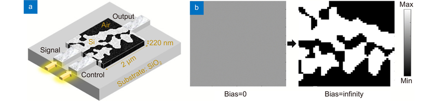
Here, we integrated two kinds of devices by inverse design method based on our improved adjoint method. The whole circuit was fabricated on Silicon-On-Insulator (SOI) with a 220-nm-thickness silicon film on 2-μm-thickness SiO2 substrate. The inverse design region was 2 μm × 2 μm × 220 nm, including 50 × 50 identical units, the size of each unit was 40 nm × 40 nm × 220 nm. Inverse design process used MATLAB to control simulation calculation through finite difference time domain software Lumerical FDTD Solutions. In the process of optimization, the refractive index of each unit continuously changed between the refractive index of silicon and air, and the final states of each unit becomed silicon or air. The circuit worked at a broad band of telecommunication C-band 1500 nm–1600 nm. Our inverse-design devices had high robustness, detailed in Supplementary information Section 1. Therefore, it also had certain robustness in the fabrication process, allowing certain fabrication error range. To simplify the calculation, we used the refractive index parameters at 1550 nm wavelength, the refractive indexes of silicon, air and substrate silica were set as
, respectively.
The objective function was set as
, whose independent variable was
. The two-dimensional cross-section electric field distribution
was a function of permittivity distribution
. Final optimized results required the distribution of the dielectric constant when the objective function meet the requirements to obtain the final structure. During the optimizing process, the dielectric constant of each unit changed continuously. Adjoint method required the dielectric constant “drop one step” along the gradient descent direction, the gradient was calculated according to the objective function, and the dielectric constant was iterated along the gradient direction, given by
Eq. (1).
where,
is the permittivity of the
iteration,
is the permittivity of the
iteration, α is the descending step,
varies between the refractive index values of Si and air,
is the gradient to be calculated, and is expressed as
Eq. (2).
where
is the equivalent signal source and
is the equivalent accompanying light source. We calculated the gradient value
of the
iteration, given by:
where
is the frequency of the signal light,
is the vacuum permeability,
is the two-dimensional cross-section electric field distribution of the accompanying light,
is the two-dimensional cross-section electric field distribution of the signal light.
is got from
and
to obtain the distribution of the dielectric constant of the
iteration. When the predetermined number of iterations is reached, ε tends to the set square value of the refractive index of Si or air, which is 3.46 or 1. The bias factor
is set to change the refractive index of each basic unit along the final gradient direction, and the speed and magnitude of the change of the refractive index are controlled according to the bias factor.
All-optical switch
Based on adjoint method, we designed an all-optical switch. The general configuration of the three-dimensional all-optical switch was shown in
Fig. 1(a), including input waveguide WG1, input waveguide WG2, inverse design structure M and output waveguide WG3. WG1 and WG2 were connected to WG3 by M. Signal light and control light were input in WG1 and WG2, respectively. The lower surface of the all-optical switch was silica substrate with a thickness of 2 μm and the background was air. M has a thickness of 220 nm, a horizontal dimension of 2 μm × 2 μm, and the two-dimensional cross-section of M was divided into 50 × 50 identical units, each of which was a 40 nm × 40 nm square with two choices: etched or unetched, that was, air or Si.
Figure 1.Design optimization process of the all-optical switch. (a) General configuration of the all-optical switch. (b) The initialization and discrete optimization permittivity distribution in the x-y two-dimensional cross-section, where bias=0 and bias=infinity.
The all-optical switch implementation was based on the principle of mode field change. In the first case, signal light was input in WG1, then transmitted in the 2 μm × 2 μm region M, and finally output in WG3. Such process corresponded to the “ON” state of the all-optical switch. In the second case, signal light was input in WG1 and at the same time, the control light was input in WG2. When two lights incident at the same time, the electric field distribution of the signal light and the control light coherently overlaid in the inverse-design area, thus changing the transmit state of the signal light. No signal output in the WG3, and such process corresponded to the “OFF” state.
We took these principles into account during the inverse design process. We got the electric field distribution E1 of the two-dimensional cross-section of M when the signal light input. According to the design requirements of device functions, we set the phase difference
between control light and signal light in the design process, and other parameters were the same. We got the electric field distribution E2 of the two-dimensional cross-section of M when the control light input. We placed an accompanying light at the output waveguide WG3, where the accompanying light was input in WG3. The parameters of the accompanying light were the same as the signal light. We got the electric field distribution
of the two-dimensional cross-section of M when the accompanying light input. Therefore, the calculated the gradient value
of the
iteration was given by:
The gradient value
of the
iteration was given by:
where
was the frequency of the signal light,
was the vacuum permeability,
was the two-dimensional cross-section electric field distribution of the accompanying light,
and
were the two-dimensional cross-section electric field distribution when the signal light and the control light input, was respectively. Therefore, we calculated the final gradient of the
iteration:
Then we got the permittivity distribution of the
iteration:
The whole optimization process can be divided into two steps: continuous optimization process and discrete optimization process. In the continuous optimization process, we set the bias factor to be small, while in the discrete optimization process, we set the bias factor to be large. The refractive index of each basic unit was optimized by using the bias factor
, which was used to control the change speed and magnitude of the refractive index. The optimization process was shown in
Fig. 1(b). After two hundred generations of iterative calculation, we got the final distribution of the dielectric constant.
Figure 1(b) shows the initialization and discrete optimization permittivity distribution when bias=0 and bias=infinity. More details were described in Supplementary information Section 2.
So far, the design work of inverse-design all-optical switch has been completed. We let signal light input in WG1, transmitted through the completed structure and output in WG3. “ON” state of the all-optical switch can be realized. The “ON” state of normalized intensity distribution in the x-y plane from theoretical calculation was shown in
Fig. 2(a). More than 30% transmittance can be achieved in a broad band of 1500 nm–1600 nm, and close to 40% transmittance can be achieved at 1550 nm, as shown in the black curve in
Fig. 2(d). Signal light was input in WG1 and at the same time, the control light was input in WG2, then transmitted through the completed structure and output in WG3. “OFF” state of the all-optical switch can be realized. The “OFF” state of normalized intensity distribution in the x-y plane from theoretical calculation was shown in
Fig. 2(b). Less than 10% transmittance can be achieved in the range of 1500-1600 nm, and close to 2% transmittance can be achieved at 1550 nm, as shown in the red curve in
Fig. 2(d). High contrast of 13 dB can be realized for the final structure.
Figure 2.Characterization of the all-optical switch. (a) The “ON” state of normalized intensity distribution in the x-y plane from theoretical calculation. (b) The “OFF” state of normalized intensity distribution in the x-y plane from theoretical calculation. (c) Scanning electron microscopy (SEM) image of the all-optical switch. The size of the optimized area was 2 μm×2 μm. (d) Simulation results of the transmission of all-optical switch. (e) Experiment results of the normalized transmission of all-optical switch. (f) The simulation and experiment results of the all-optical switch ON/OFF contrast.
The principle of our design is that the signal light and control light work together at the output waveguide to reduce the transmittance of the signal light. Light propagated in the inverse-design area is affected by the structure of each 40 nm × 40 nm unit. We need the signal light and control light interference at the output waveguide, thus eliminating the signal light, so the structure is dissymmetry in the Y direction, resulting in a large transmittance difference between the input states of “10” and “01”. We also calculated other configurations that can improve the signal light transmittance, but the transmittance of “11” state increased at the same time. For we only need to pay attention to the situation of signal light inputs, after considering all the calculated results, we chose such a configuration in
Fig. 1(b), which had more than 10 dB “ON” and “OFF” contrast.
The devices were fabricated by using beam lithography followed by inductively coupled plasma (ICP) etching, as detailed in Method. Scanning electron microscopy (SEM) images of a final fabricated device was shown in
Fig. 2(c). The all-optical switch was measured using an optical fiber coupling system (see Method). The experiment results were shown in
Fig. 2(e). The measured average transmission of 1500 nm-1600 nm of the “ON” state was 40% and the maximum value was 48%, as shown in the black line in
Fig. 2(e). The measured average transmission of the “OFF” state was 5% and the maximum value was 9%, as shown in the red line in
Fig. 2(e). Our inverse-design all-optical switch had a higher ON/OFF contrast over 8 dB theoretically, up to 10 dB, as shown in the black curve in
Fig. 2(f) and over 6 dB experimentally, up to 10 dB, as shown in the red curve in
Fig. 2(f), which was in agreement with the theoretical results.
To study the time response property, we calculated the transmission of the all-optical switch with a different time delay of the signal light and the control light.
Fig. 3(a) shows the normalized intensity distribution of 1550 nm in the x-y plane from theoretical calculation when the time delay was 0 fs, where the electric field intensity of the output waveguide was low, corresponding to the “OFF” state.
Fig. 3(b) shows the intensity distribution when the time delay was 40 fs, output field intensity was larger than 0 fs.
Fig. 3(c) and
3(d) show the normalized intensity distribution when the time delay was 80 fs and 100 fs, respectively. Transmission of the all-optical switch under different delay time at 1500 nm–1600 nm is shown in
Fig. 3(e). We also gave the transmission under different delay time at 1500 nm, as shown in
Fig. 3(f). We concluded that when the time delay was 80 fs, it achieved the highest value compared with 0 fs, 40 fs and 100 fs time delay. The electric field intensity of the output waveguide in
Fig. 3(b–d) was high, corresponding to the “ON” state. At different working wavelengths, the conversion time of “ON” state to “OFF” state, was different but within hundred femtoseconds. According to the simulated results, when the time delay is 100 fs, the switch can achieve a maximum switching contrast of 13 dB. The response time meets the requirements of ultrafast information processing in need. To realize the all-optical switch, the intensity of the control light was as low as that of the signal light, the all-optical switch with ultra-low energy consumption can be realized.
Figure 3.Characterization of the all-optical switch. (a) The “OFF” state of normalized intensity distribution in the x-y plane from theoretical calculation at t=0 fs. (b–d) The “ON” state of normalized intensity distribution in the x-y plane from theoretical calculation at t=40 fs, 80 fs and 100 fs, respectively. (e) Transmission of the output of the all-optical switch under different delay time at 1500 nm-1600 nm. (f) Transmission of the output of the all-optical switch under different delay time at 1500 nm.
The general configuration of the three-dimensional all-optical XOR logic gate was shown in
Fig. 4(a), including input waveguide WG1, input waveguide WG2, inverse-design structure M and output waveguide WG3. WG1 and WG2 were connected to WG3 by M. To facilitate the integration of the whole device and the transmission of light in the inverse design region, two incident waveguides were placed in two symmetrical positions above and below the inverse-design area. Signal light Signal1 and signal light Signal2 were input in WG1 and WG2, respectively. The design process of the all-optical XOR logic gate was detailed in Supplementary information Section 3.
Figure 4.Design optimization process of all-optical XOR logic gate. (a) General configuration of the all-optical XOR logic gate. (b) The initialization and discrete optimization permittivity distribution in the x-y two-dimensional cross-section, where bias=0 and bias=infinity.
In the first case, no signal input and no electric field output, corresponding to the ‘0’ XOR ‘0’=‘0’ operation of the all-optical XOR logic gate. In the second case, signal light Signal1 was input in WG1, light was transmitted in the 2 μm × 2 μm region M, and strong signal light outputs in WG3, corresponding to the ‘1’ XOR ‘0’=‘1’ operation of the all-optical XOR logic gate. The normalized intensity distribution in the x-y plane from theoretical calculation was shown in
Fig. 5(a). The calculated transmission was shown in the black line in
Fig. 5(e). More than 30% transmittance can be achieved in the ultra-wideband wavelength range of 1500 nm–1600 nm, and close to 40% transmittance can be achieved at a 1550-nm working wavelength. In the third case, signal light Signal2 was input in WG2, light was transmitted in M, and strong signal light outputs in WG3, corresponding to the ‘0’ XOR ‘1’=‘1’ operation of the all-optical XOR logic gate. The normalized intensity distribution in the x-y plane from theoretical calculation was shown in
Fig. 5(b). The calculated transmission was shown in the red line in
Fig. 5(e). More than 10% transmittance can be achieved in the ultra-wideband wavelength range of 1500 nm-1600 nm, and close to 25% transmittance can be achieved at a 1550-nm working wavelength. In the fourth case, signal light Signal1 and signal light Signal2 were input in WG1 and WG2 and weak signal light output in WG3. When two signal lights incident at the same time, the electric field distribution in the inverse-design area was a linear superposition, the output signal was weak, corresponding to the ‘1’ XOR ‘1’=‘0’ operation of the all-optical XOR logic gate. The normalized intensity distribution in the x-y plane from theoretical calculation was shown in
Fig. 5(c). Calculated transmission was shown in the blue line in
Fig. 5(e). Less than 10% transmittance can be achieved in the ultra-wideband wavelength range of 1500 nm–1600 nm, and close to 2% transmittance can be achieved at a 1550 nm working wavelength.
Figure 5.Characterization of the all-optical XOR logic gate. (a) The “01” input of normalized intensity distribution in the x-y plane from theoretical calculation. (b) The “10” input of normalized intensity distribution in the x-y plane from theoretical calculation. (c) The “11” input of normalized intensity distribution in the x-y plane from theoretical calculation. (d) Scanning electron microscopy (SEM)image of the XOR logic gate. The size of the optimized area was 2 μm×2 μm. (e) Simulation results of the transmission of all-optical switch. (f) Experiment results of the normalized transmission of all-optical XOR logic gate.
The devices were fabricated by using electron beam lithography followed by inductively coupled plasma (ICP) etching, as detailed in Section Method. Scanning electron microscopy (SEM) images of a final fabricated device was shown in
Fig. 5(d). The all-optical XOR logic gate was measured using an optical fiber coupling system (see Supplementary information S1.2). The experiment result was shown in
Fig. 5(f). The measured average output transmission of ‘0’ XOR ‘1’=‘1’ operation was 40% and the maximum value was 48%, as shown in the black line in
Fig. 5(f). The measured average output transmission of ‘1’ XOR ‘0’=‘1’ operation was 20% and the maximum value was 35%, as shown in the red line in
Fig. 5(f). The different transmission results of ‘0’ XOR ‘1’=‘1’ operation and ‘1’ XOR ‘0’=‘1’ operation originate from the asymmetry of the inverse-design structure. The measured average output transmission of ‘1’ XOR ‘1’=‘0’ operation was 3%, as shown in the blue line in
Fig. 5(f). Our inverse-design all-optical XOR logic gate has a higher ‘1’/’0’ contrast over 15 dB theoretically and experimentally.
For all-optical XOR logic gate, we only need to control the phase and intensity of the two signal lights identical, so we define the propagation time of the light in the structure as the response time of the XOR logic gate. The footprint of a single device was 2 μm × 2 μm, so for the all-optical XOR logic gate, the propagation time of the signal light was the response time of the optical XOR logic gate based on the linear light principle. The theoretical response time was 23 fs.
High performance integrated photonic circuit
Our expective integrated photonic circuit includes the inverse-design all-optical switch and all-optical XOR logic gate, using the all-optical switches to control the input states of the XOR logic gate. We have considered the crosstalk among the devices during the design process. The purpose was to let the output transmission of the all-optical switch in the integrated photonics circuit equal to the single all-optical switch. Based on that, we could easily solve the crosstalk problem through inverse design method. The corresponding improved process was that we add two monitors to compare the output transmission difference of the integrated and single all-optical switch in the inverse design algorithm and at the same time, we ensure the high output transmission of the ‘1’ XOR ‘0’=‘1’ and ‘0’ XOR ‘1’=‘1’ operation of the XOR logic gate to lower the crosstalk indirectly.
Figure 6(a) shows the circuit, including Switch1, Switch 2 and XOR logic gate. Signal light Signal1, signal light Signal2 and two control lights were input in corresponding waveguides. Switch1 includes input waveguide WG1, input waveguide WG2, inverse design structure M1 and connected waveguide WG3. Switch2 includes input waveguide WG4, input waveguide WG5, inverse design structure M2 and connected waveguide WG6. XOR logic gate includes connected waveguide WG3, connected waveguide WG6, inverse design structure M3 and output waveguide WG7. The overall working state was shown in
Table 1. There were four cases in the circuits. The “ON” state of the all-optical switch was corresponding to the logic state of ‘1’ and the “OFF” state of the all-optical switch was corresponding to the logic state of ‘0’. In the first case, the states of Switch1 and Switch2 were both “OFF”, corresponding to the input logic state of XOR logic gate of both ‘0’. In the second case, the state of Switch1 was “ON” and Switch2 was “OFF”, corresponding to the input logic state of XOR logic gate of ‘1’ and ‘0’. In the third case, the state of Switch1 was “OFF” and Switch2 was “ON”, corresponding to the input logic state of XOR logic gate of ‘0’ and ‘1’. In the fourth case, the states of Switch1 and Switch2 were both “ON”, corresponding to the input logic state of XOR logic gate of both ‘1’.
Figure 6.Characterization of the all-optical integrated circuit.(a) General configuration of the all-optical integrated circuit. (b) The “11” input (“ON” and ”ON” states) of normalized intensity distribution in the x-y plane from theoretical calculation. (c) The “10” input (“ON” and ”OFF” states) of normalized intensity distribution in the x-y plane from theoretical calculation. (d) The “01” input (“OFF” and ”ON” states) of normalized intensity distribution in the x-y plane from theoretical calculation. (e) The “00” input (“OFF” and ”OFF” states) of normalized intensity distribution in the x-y plane from theoretical calculation.
Normalized intensity distribution in the x-y plane from theoretical calculation of the four cases were shown in
Fig. 6(b)–6(e). There was almost no energy output at the output waveguide, as shown in
Fig. 6(b, e). Compared with the above case, there was a significant energy output at the exit waveguide, as shown in
Fig. 6(c, d). The feature size of the whole circuit was only 2.5 μm × 7 μm, as shown in SEM images in
Fig. 7(a). The distance between two adjacent devices was as small as 1.5 μm, within wavelength magnitude scale. Such features provide a nice platform for high-density photonic integration research. Our integrated circuit achieves a very high contrast signal processing. Simulation results and experiment results of the transmission of the all-optical integrated circuit were shown in
Fig. 7(b) and
7(c), respectively. Four color curves were corresponding to the above four cases. Such all-optical integrated circuit can achieve a transmittance of more than 7% at 1550 nm when the input states are “1011” and “1110”, it can also achieve a high “0” and “1” contrast of more than 10 dB at 1550 nm. The experimental results were consistent with the simulation results.
Figure 7.Characterization of the all-optical integrated circuit. (a) Scanning electron microscopy (SEM) image of the all-optical integrated circuit. The size of the optimized area was 2.5 μm×7 μm. (b) Simulation results of the transmission of the all-optical integrated circuit. (c) Experiment results of the normalized transmission of the all-optical integrated circuit.
The theoretical response time of the all-optical switch was 80 fs, and the threshold energy of control light was 10 fJ/bit, equal to the signal light for the all-optical switch, detailed calculation process was shown in Section Measurement. The response time of the logic gate was 23 fs. Therefore, the whole response time was less than 150 fs and the energy consumption was within 10 fJ/bit. Because the scattering loss of the device itself was very small, the light can be confined to the optical transmission device structure, so this ultra-compact integrated connection method brings very little loss. The loss of light comes from the inevitable loss in the optical operation process, as detailed in Section Method.
Moreover, we consider the crosstalk through the whole optimizing process of integrated circuit, thus overcoming the crosstalk problem. We placed two monitors to compare the output transmission difference of the integrated and single all-optical switch in the inverse design algorithm. At the same time, we ensured the high output transmission of the ‘1’ XOR ‘0’=‘1’ and ‘0’ XOR ‘1’=‘1’ operation of the XOR logic gate to lower the crosstalk indirectly. The reflected energy of adjacent device would affect the energy transmission in the connected waveguide.
Our integrated photonic circuit also realizes the function of identifying whether two two-digit numbers were equal or not. When logic signal 1 was equal to logic signal 2, the identifying result of the circuit was 0. When logic signal 1 was different from logic signal 2, the identifying result of the circuit was 1. Such function plays an important part in logic information processing, as shown in
Table 2.
Table Infomation Is Not Enable
Conclusions
We realized an ultra-compact integrated photonic circuit composed of three devices with two all-optical switches controlling the input states of an XOR logic gate by using the improved inverse-design method. The whole circuit was only 2.5 μm × 7 μm, a single device was 2 μm × 2 μm and the distance of each device was 1.5 μm. We use the principle of mode field change and the whole design process was based on the improved adjoint method. The theoretical response time of the integrated photonic circuit was within 150 fs. The threshold intensity of control light was equal to the signal light for the all-optical switch, within 10 fJ/bit. Our work provides a new idea for the design of ultrafast and ultra-low energy consumption all-optical devices and the implementation of high-density and on-chip integrated photonic circuits.
Method
Matrix representation of optical devices
An optical device has
input ports and
output ports(some ports may be both input and output). Devices made of linear materials, the electric field at the output ports and the input ports of which are related by Matrix:
where,
represents the electric field at
input waveguides,
represents the electric field at
output waveguides.
are all complex numbers, which can be abbreviated as
Here we consider only the waveguide fundamental mode(or near) transmitted in the input or output waveguide. The total input power was normalized:
The limitation of energy conservation
Due to the limitation of energy conservation, not any matrix
can be realized. The output power cannot become larger than 1:
We define
. It was easy to prove that
was Hermitian (
). All
eigenvalues of
are real and positive semidefinite. Conservation of energy was satisfied if the maximum eigenvalue of
was less than or equal to 1. We can also represent it in terms of the norm of the following matrix:
of
Eq. (12) was achievable.
‘XOR’ gate
The analytical process was not very different from the ‘OR’ gate case. The matrix can be written as
If only one input port has incident light, the transmission was only 50%. Only when two ports simultaneously incident the lights with the same amplitude and have a phase difference of
, the device was lossless. We can prove that any device with
less than
, cannot meet the lossless condition.
Fabrication
We first clean SOI piece (2 cm × 2 cm) at 70 °C both DSF-2 and DQY-2 bath for 60 min. The integrated photonic devices and waveguides were defined by patterning a 250 nm ZEP-520A resist layer using JEOL JBX-9500FS electron beam lithography system. The etching process of silicon device layer uses equipment OXFORD PlasmaPro 100 Cobra 180. Then we strip resist in 70 °C DQY-2 baths for 30 min. At this point, the whole device preparation process was over.
Measurement
The scanning electron microscopy (SEM) image of the completed device was analyzed through Zeiss GeminiSEM 500. We measure the linear transmission spectrum of the devices using an optical fiber coupling system. During the whole measurement, a super continuous laser (YSL SC-5) was used to excite the signal light from the single-mode fiber. The intensity of the signal light was adjusted by adjusting three polarizers, and then the signal light was focused on the coupling fiber. The optical fibers are placed on a precise three-dimensional displacement table. We optimize the near-field coupling with the grating coupler by carefully adjusting the position and angle of the incident fiber. Another single-mode fiber was symmetrically placed at the output coupling end of the grating coupler to collect the output signal light through near-field coupling. We normalized transmission by using reference samples with the same grating coupler parameters but no nano-structures.
The parameters of the super continuous laser are: maximum output power of was 800 mW, peak output power output from the optical fiber was 100 μW, central wavelength was 1064 nm, repetition frequency was 5 MHz, the pulse width was 400 ps and the power ratio of 1550 nm was 0.001. The coupling efficiency of the grating was 10%. Therefore, the energy of 1550 nm signal light and control light was calculated as 2 fJ /bit。