
Tae-Woo Lee, Dohong Kim, Jun Hee Han, Somin Lee, Hoseung Lee, Seungyeop Choi, Kyung Cheol Choi. Suppressing surface plasmon losses to improve the efficiency of blue organic light-emitting diodes using the plasmonic quasi-bandgap phenomenon[J]. Photonics Research, 2021, 9(9): 1784
- Photonics Research
- Vol. 9, Issue 9, 1784 (2021)
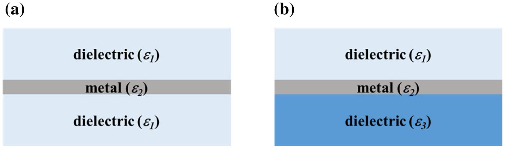
Fig. 1. Schematic of (a) symmetric and (b) asymmetric DMD waveguides.
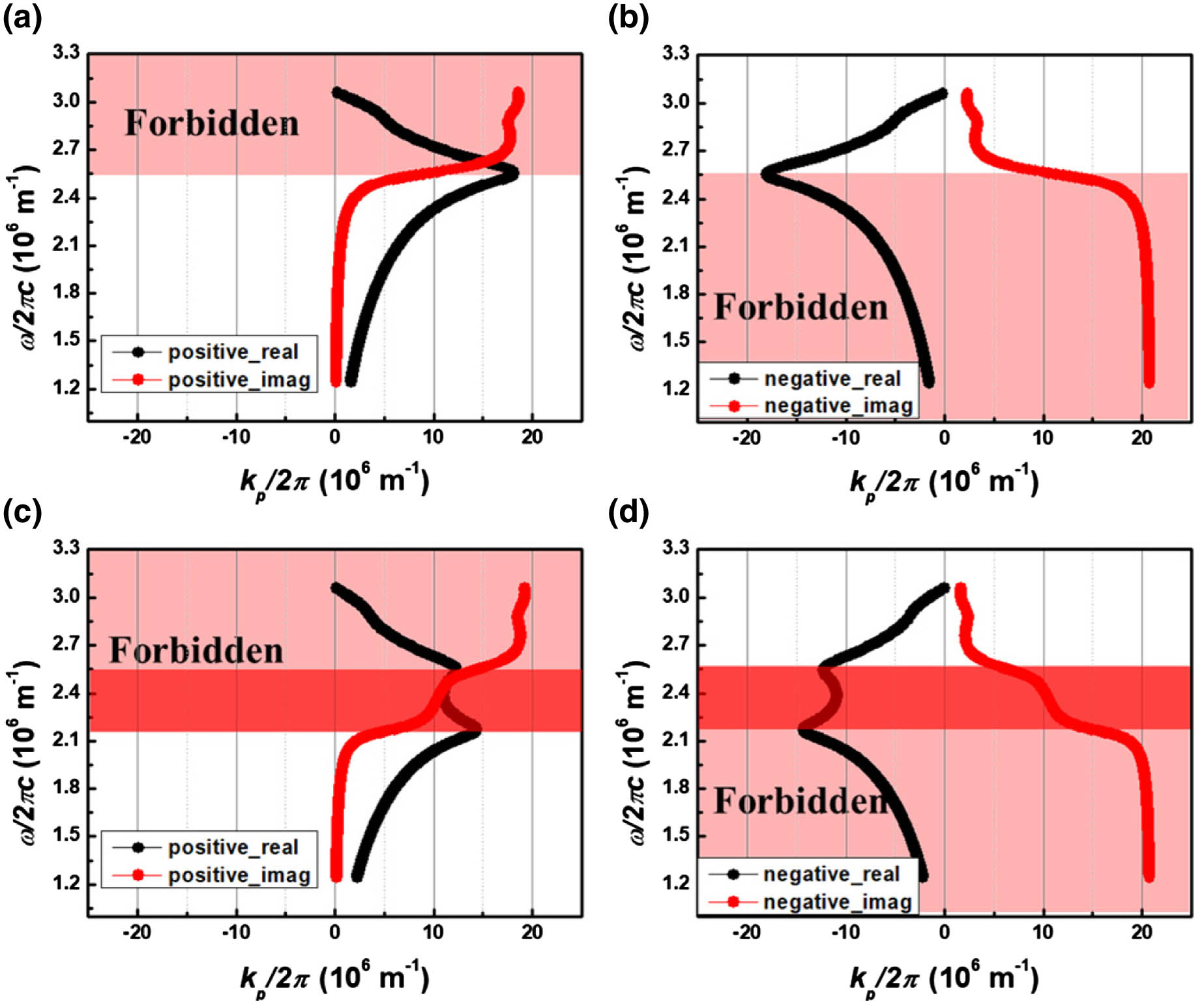
Fig. 2. Dispersion relation of the (a), (b) symmetric and (c), (d) asymmetric waveguides. (a) and (c) are even plasmonic waveguide modes. (b) and (d) are odd plasmonic waveguide modes.
Fig. 3. Electric field profiles of waveguides using FDTD simulation. (a) Simulation structure, and mode profile of the (b) symmetric DMD waveguide and (c) asymmetric DMD waveguide.
Fig. 4. (a) Thickness of each layer, used to determine the microcavity in a thin Ag film DMD electrode; (b) spectral intensity of the capping layer thickness at 460 nm wavelength; spectral intensity according to wavelength at optimized (c) NPB and (d) ZnS capping layer thicknesses.
Fig. 5. Inverted top emission OLED structure. Schematic of (a) OLEDs with symmetric DMD electrode and (b) OLEDs with asymmetric DMD electrode; (c) and (d) their FIB-SEM images.
Fig. 6. Electrical and optical properties of the inverted top emission OLED devices with symmetric/asymmetric DMD electrodes. (a) Current density-voltage; (b) luminance-current density; (c) efficacy-current density; and (d) EL spectrum.
Fig. 7. (a) Calculated spectral power density at a wavelength of 460 nm for the symmetric and asymmetric DMD electrodes with respect to the normalized in-plane wave vector and (b) its spectral power density ratio; (c) total power ratio of both electrodes in a study considering the Purcell effect.
Fig. 8. Transparent OLED structure. Schematic of transparent OLED with (a) ITO anode and asymmetric DMD cathode, and (b) both asymmetric DMD electrodes; (c) luminous transmittance of (a), and (d) luminous transmittance of (b) with respect to the ZnS thickness; (e) measured transmittance of (a), and (f) measured transmittance of (b). Insets of (e) and (f) indicate photographs of the transparent OLED with on/off images.
Fig. 9. Electrical and optical properties of the transparent OLED devices with ITO/asymmetric DMD electrodes. (a) Current density-voltage; (b) luminance-current density; (c) efficacy-current density; (d) EQE-current density; (e) power efficiency-current density; and (f) normalized EL spectrum.
Fig. 10. (a) Calculated spectral power density at a wavelength of 460 nm for the ITO and asymmetric DMD electrodes with respect to the normalized in-plane wave vector; (b) total power ratio of both electrodes in an analysis considering the Purcell effect.
Fig. 11. Flexibility of proposed transparent OLED. (a) Sheet resistance ratio of each electrode with respect to number of bendings. Inset of (a) indicates bending strain. Photograph of flexible transparent OLED with (b) off and (c) on images.
| ||||||||||||||||||||||||||||||||||||||||||||||||||||||||||||||||||||||||||||||||||||||||
Table 1. Summarizing Device Labels and Their Thicknesses

Set citation alerts for the article
Please enter your email address
© Copyright 2018-2021 | Chinese Laser Press. All Rights Reserved 沪ICP备15018463号-20