
Tae-Woo Lee, Dohong Kim, Jun Hee Han, Somin Lee, Hoseung Lee, Seungyeop Choi, Kyung Cheol Choi. Suppressing surface plasmon losses to improve the efficiency of blue organic light-emitting diodes using the plasmonic quasi-bandgap phenomenon[J]. Photonics Research, 2021, 9(9): 1784
- Photonics Research
- Vol. 9, Issue 9, 1784 (2021)
Abstract
1. INTRODUCTION
The demand for organic light-emitting diodes (OLEDs) for various applications is increasing, and as a result the overall market is growing [1–5]. Market trends are also shifting from liquid crystal displays (LCDs) to displays using OLEDs. But in spite of their bright prospects in next-generation displays with spontaneous emission and no backlight, OLEDs still have some challenges to overcome. Among other things, when the device is driven with high luminance, it exhibits relatively low efficiency or poor lifetime compared with LCD devices, and this should be improved. In addition, to accurately represent all the colors of nature, it must be able to express the three elements of red, green, and blue clearly and efficiently [6].Thus far, materials and structures have been developed with high efficiency for red and green, but blue has not yet achieved the efficiency and stability of those other color elements [7]. Therefore, for the commercial success of OLED displays, research to improve the efficiency of blue devices for use in the next-generation display is very important.
To improve the efficiency of blue devices, efforts to develop materials with first-generation fluorescence have been expanded, with the development of materials with second-generation phosphorescence, third-generation thermally activated delayed fluorescence, and fourth-generation hyperfluorescence. A number of studies have subsequently been published confirming significant improvements in blue OLED efficiency when utilizing materials from the second generation to the fourth generation, compared to first-generation fluorescent devices [8–13]. However, they are still far from being commercialized in terms of device stability, reliability, and cost-effectiveness.
In addition to material development, many studies have also been carried out using optical structure design. The goal of these efforts is to increase outcoupling efficiency to improve the light extraction of OLEDs [14–21]. There are three main approaches used to improve light extraction efficiency by optical structural design. The first method is to extract the light confined in the substrate by modifying the external structure of the device. The second is to extract the waveguide loss mode or surface plasmon loss mode by inserting a light extracting structure into the device. The third uses a microcavity structure to generate cavity resonance. Although each method has advantages, there are also disadvantages, and this makes it necessary to propose a modified structure.
Sign up for Photonics Research TOC. Get the latest issue of Photonics Research delivered right to you!Sign up now
In this paper, we propose a new theory to improve the efficiency of blue OLEDs, not just from the materials point of view but from the optical point of view, and we then analyze the characteristics of the realized device. We used blue fluorescent light-emitting materials that are presently being used in industry and propose a structure that can take advantage of the conventional microcavity structure and overcome its limitations. We also propose a highly efficient transparent blue OLED based on a plasmonic quasi-bandgap (PQB).
2. RESULT AND DISCUSSION
A. PQB at Visible Wavelength
Recently, research determined the existence of a PQB region in an asymmetric dielectric/metal/dielectric (DMD) plasmonic waveguide using aluminum (Al)-doped zinc oxide (AZO). It had a negative dielectric constant value in the infrared region [22]. According to the study, surface plasmon polaritons (SPPs) are not allowed in the PQB region, and light is radiated to the outside of the waveguide. When this PQB characteristic is applied in an OLED, the light emitted from the exciton is not coupled to the SPP but radiates to the outside, thus improving light extraction efficiency. If the PQB region formed in the infrared region can be brought into the visible wavelength region, especially blue wavelengths, it is expected that the loss channel caused by the surface plasmon can be reduced.
Figures 1(a) and 1(b) show symmetric and asymmetric DMD waveguides made of a metal thin film sandwiched between two dielectric materials. In the symmetric waveguide, the two materials have the same dielectric constant, and in the asymmetric one, the materials have different dielectric constants. The PQB region is determined by the type of metal and dielectric materials [22]. Silver (Ag), copper, and gold are prime candidates for forming a PQB in the visible wavelength region using sandwiched metal.
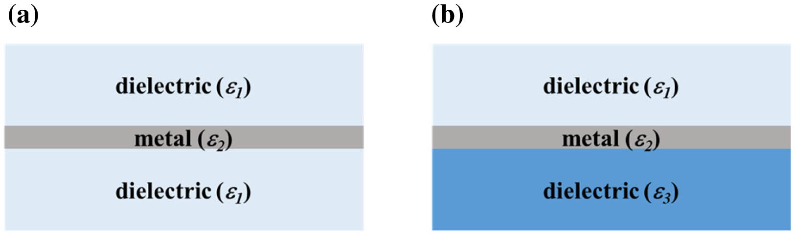
Figure 1.Schematic of (a) symmetric and (b) asymmetric DMD waveguides.
In this study, Ag, which has the advantages of work function as well as cost-effectiveness as an OLED electrode, was selected as the metal thin film.
To investigate the PQB characteristics of the asymmetric DMD electrode, the electrode was considered to be an effective waveguide. The dispersion relation of the symmetric DMD waveguide, which utilized upper and lower materials with the same dielectric constant, was used as a reference and compared with the dispersion relation of the asymmetric DMD waveguide to determine whether surface plasmon loss occurred in the electrode. The dispersion relation of the plasmonic waveguide in the DMD structure is as follows [22]:
From the above dispersion relation, it can be seen that the dispersion characteristic is greatly changed in the frequency (wavelength) region where the dielectric constant value is or . The critical point, where the dispersion characteristic is changed, is calculated from the dielectric constant of the organic layer, metal layer, and capping layer of the DMD electrode. In general, the refractive index of the organic materials in OLEDs is about 1.8. When Ag is used as the metal layer, this corresponds to a significant change in the dispersion relation in the region below a wavelength of 400 nm. Therefore, for the PQB to exist in the desired wavelength range, the capping layer material must have a high refractive index. And for the convenience of fabrication, it is necessary to select a material that can be simply deposited by vacuum thermal evaporator. Zinc sulfide (ZnS), a representative material with a large refractive index that can be deposited by vacuum thermal evaporation, was selected as the capping layer of the asymmetric DMD electrode. The thickness of Ag is set to 12 nm, and the thickness of both dielectric materials is set to infinite. The refractive indices of the Ag, the organic materials, and ZnS used in the electrode were measured by ellipsometry, and the dielectric constant was calculated based on the measurement data.
Figures 2(a) and 2(b) represent the dispersion relation when the outer capping layer of the DMD electrode is a material with the same dielectric constant as the internal organic material (symmetric). Figures 2(c) and 2(d) show the dispersion relation when the outer capping layer of the DMD electrode is ZnS with a high refractive index (asymmetric), where is a wave vector defined as . In the symmetric DMD structure shown in Figs. 2(a) and 2(b), the imaginary part of the plasmonic wave vector rises rapidly near the 410 nm wavelength region. In these high damping regions, propagation of the surface plasmon is prohibited, and light is radiated to the outside. Therefore, the positive index plasmonic mode is suppressed in wavelength regions shorter than 410 nm, and the negative index plasmonic mode is suppressed in wavelength regions longer than 410 nm.
![]()
Figure 2.Dispersion relation of the (a), (b) symmetric and (c), (d) asymmetric waveguides. (a) and (c) are even plasmonic waveguide modes. (b) and (d) are odd plasmonic waveguide modes.
A positive index plasmonic mode and a negative index plasmonic mode also appear in the asymmetric DMD waveguide. However, unlike the dispersion relationship in the symmetric DMD waveguide, it can be seen that the imaginary part of the dispersion relation changes to a step-like mode as the wavelength is changed. As a result, the forbidden areas of the positive index mode and the negative index mode overlap each other, and this area is called the PQB. At this time, the PQB wavelength ranges from 410 to 470 nm, and includes 460 nm, which is the desired blue OLED peak wavelength.
A numerical simulation based on finite-difference time-domain (FDTD) was conducted to verify the electric field profiles of the symmetric and asymmetric DMD waveguides. After applying a monochromatic dipole source with a target wavelength of 460 nm, the SPP waveguide mode was examined. The simulation employed a two-dimensional structure, as shown in Fig. 3(a). The symmetric DMD waveguide used the same refractive index as the -bis(naphthalen-1-yl)- -bis(phenyl)benzidine (NPB) material in the upper and lower dielectric layers, while the asymmetric DMD waveguide used the refractive index of ZnS and NPB, and the refractive index of Ag was used for the metal layer. To determine the mode profile in an ideal DMD plasmonic waveguide, the thickness of the dielectric layer was set to 1 μm, and the and boundary conditions were set to a perfectly matched layer. Since the surface plasmon is only generated in the transverse magnetic mode, a vertical dipole was used as the source, and the field monitor was calculated to be a distance of 1 μm from the source. Because the Ag film is very thin (12 nm), the mesh size was set to 1 nm for accurate calculation.
![]()
Figure 3.Electric field profiles of waveguides using FDTD simulation. (a) Simulation structure, and mode profile of the (b) symmetric DMD waveguide and (c) asymmetric DMD waveguide.
Figures 3(b) and 3(c) show the electric field distribution when a vertical dipole source is applied 1 μm away from the symmetric DMD waveguide composed of NPB/Ag/NPB, and an asymmetric DMD waveguide composed of NPB/Ag/ZnS, respectively. In the symmetric DMD waveguide, Fig. 3(b) shows that the SPP propagates along the interface between the metal and the dielectric. On the other hand, in the asymmetric DMD waveguide, Fig. 3(c), no photonic mode exists along the metal and dielectric interface. At this point, it can be seen that the electromagnetic wave emitted from the dipole source is due to radiational loss and is not coupled to the SPP in terms of the plasmonic waveguide (
B. PQB-Based Microcavity OLED
The microcavity OLED structure proposed in this paper is based on an asymmetric DMD electrode, which can reduce the losses caused by surface SPPs without inserting internal structures. Its purpose is to improve the light extraction efficiency and color purity of the conventional microcavity structure. The waveguide structure was analyzed theoretically to determine how SPP loss is reduced by the asymmetric DMD electrode. The device was fabricated, and its improved efficiency was confirmed.
Various types of electrode materials and structures, including transparent conducting oxides [23], metal nanowires [24], graphene [25], conducting polymers [26], and multilayered thin-film metals [27–31], can be utilized in OLEDs depending on their purpose and application. In this work, among various electrode structures, a multilayered thin-film structure containing metal was selected. This structure allows the manipulation of the microcavity effect, improving the optical efficiency of the blue fluorescent OLED without additional internal or external structures, as shown in Fig. 4(a). The electrode structure included metal at both ends of the OLED electrode.
![]()
Figure 4.(a) Thickness of each layer, used to determine the microcavity in a thin Ag film DMD electrode; (b) spectral intensity of the capping layer thickness at 460 nm wavelength; spectral intensity according to wavelength at optimized (c) NPB and (d) ZnS capping layer thicknesses.
Since the optical resonance phenomenon and the loss mode by SPP occur simultaneously, it is important to minimize losses due to surface plasmons while maximizing the resonance effect. Accordingly, the thin-film asymmetric DMD electrode, which forms a PQB in the blue wavelength region, was selected as the structure to optimize the cavity resonance and reduce surface plasmon loss,
In the OLED structure using the microcavity effect, the resonance effect is largely determined by two factors [21]. The first is the interference effect caused by the phase difference between the light directly emitted from the emission layer (EML) and the reflected light at the reflector, which is called two-beam interference. The second is called the Fabry–Perot interference factor, which is produced by the multiple reflections between both electrodes. By multiplying these two factors, the cavity gain can be obtained.
Equations (3)–(5) represent the two-beam interference factor, Fabry–Perot factor, and cavity gain, respectively. Each factor in the equation represents the transmission coefficient (), the reflection coefficient (), the phase difference, the distance between the EML and the reflector (), and the cavity length (), respectively. For multilayer thin films such as OLEDs, multiple reflections by each layer should be taken into account when determining the factors in the above equation. The matrix method is typically used to calculate this [32]. Finally, Eq. (5) can be used to determine the resonant wavelength of the microcavity structure.
Figure 4(a) shows the three factors that determine the resonant wavelength in the inverted top emitting OLED proposed in this paper. In general, OLED devices that use the microcavity effect employ a relatively thick metal of 30 nm or more as an electrode. Unlike these typical microcavity devices, using a 12 nm thin metal film electrode will have a significant effect on the reflectivity and phase difference, via the thickness and refractive index of the external capping layer, resulting in a change in cavity wavelength.
Therefore, after optimizing and optically and electrically by using a relatively thick Ag film of 30 nm, simulations and experiments were conducted to optimize the thickness of the capping layer by controlling the material and the thickness. In the previously reported blue OLED device using indium tin oxide (ITO) as an electrode, the thickness of the organic layer had to be reduced because the cavity length was larger than the blue wavelength of 460 nm [8]. Among the organic layers in the OLED structure, except for the EML and hole transport layer (HTL), the other layers were so thin that the thickness hole injection layer (HIL), electron injection layer (EIL), and electron transport layer (ETL) could not be adjusted further, so the thicknesses of the EML and HTL had to be adjusted.
The optimized thicknesses of the EML and HTL were calculated to be 25 and 45 nm, respectively. However, when the internal thickness of the OLED is changed, the charge balance may also be changed, depending on the change in the thickness of each functional layer. Therefore, before fabricating an MADN:DSA-Ph-based blue fluorescent OLED using a microcavity structure, it is necessary to check whether the charge balance is maintained when the thickness of the organic material is modified to the resonance wavelength.
After the internal organic structure was set up, a device with reduced HTL and EML thickness was fabricated to confirm that the charge balance was consistent with the reported reference device. It was confirmed that the charge balance was maintained even when the HTL and EML thicknesses were changed to 45 and 25 nm, respectively. Finally, the asymmetric DMD electrode, which can reduce SPP loss in the OLED device by using PQB, was optimized. ZnS was used as the capping layer of the asymmetric DMD structures, as mentioned above.
As a reference device for the asymmetric DMD electrode, a symmetric DMD structure using NPB as the capping layer was fabricated, and the two devices were compared. Figure 4(b) shows the spectral intensity according to the change in NPB and ZnS thicknesses when used as a capping layer at 460 nm wavelength, as calculated by cavity simulation. It shows the spectral intensity at the optimal point. The ZnS capping layer showed the highest spectral intensity of around 70 nm, and the NPB was optimized at around 85 nm. Figures 4(c) and 4(d) show the , , and values of the NPB and ZnS capping layers, respectively, at each optimization point.
Optimized blue OLED devices were fabricated to confirm that the asymmetric DMD electrode contributed to the improvement in light extraction efficiency by reducing losses caused by surface plasmons. Figures 5(a) and 5(b) show the structure of the inverted top emission OLED devices, which include the symmetric/asymmetric DMD electrodes. The light-emitting layer used in this study was fabricated by the codeposition of -bis(-diphenyl-aminostyryl)benzene (DSA-Ph), a styrylamine type dopant, on the 2-methyl-9,10-di(2-napthyl)anthracene (MADN) host material. As reported in a previous study, codeposition was performed at a molar ratio of 3%, and NPB and tris(8-quinolinolato)aluminium () materials were used as the HTL and ETL materials, respectively.
![]()
Figure 5.Inverted top emission OLED structure. Schematic of (a) OLEDs with symmetric DMD electrode and (b) OLEDs with asymmetric DMD electrode; (c) and (d) their FIB-SEM images.
As the HIL and EIL materials, molybdenum trioxide () and lithium-8-hydroxyquinolinolate (Liq), which have characteristics similar to materials in a previous study and are widely used, were additionally used. Al was used as the cathode. A symmetric DMD electrode was used as a reference anode, and performance was then compared to an OLED device using an asymmetric DMD electrode. The devices were fabricated using the inverted top emitting structure.
Figures 5(c) and 5(d) show a focused ion beam scanning electron microscope (FIB-SEM) image of a cross section of the fabricated devices. As can be seen from the figures, all thicknesses except the capping layer are identical. The material deposited 100 nm above the NPB and ZnS on the FIB-SEM images is a Ag layer, which acts as a buffer layer to prevent the NPB layer from being cut off along with the carbon coating when the device is being cut by the focused ion beam. It does not exist in the actual fabricated devices.
Figure 6 shows the characteristics of the blue fluorescent OLEDs utilizing the symmetric and asymmetric DMD electrodes. The relationship between current density and voltage is shown in Fig. 6(a). No significant difference can be seen between the devices, and the electrical characteristics are almost identical. This is the case because all of the layers except the capping layer are the same, so they do not affect the electrical characteristics of the device.
![]()
Figure 6.Electrical and optical properties of the inverted top emission OLED devices with symmetric/asymmetric DMD electrodes. (a) Current density-voltage; (b) luminance-current density; (c) efficacy-current density; and (d) EL spectrum.
On the other hand, as shown in Fig. 6(b), luminance is higher in the device using the asymmetric electrode structure at the same current density. This confirms the improvement in light extraction efficiency. The current efficiency was 15% higher at the same current density, as shown in Fig. 6(c). Figure 6(d) provides the electroluminescence (EL) spectra and a cell image of each device at a driving voltage of 4.5 V. In terms of EL spectra, a reduction in the shoulder peak of 500 nm was observed in the OLED with the asymmetric DMD electrode structure. Compared to the relative EL spectra, it showed that the efficiency at the target wavelength of 460 nm was improved.
Meanwhile, the PQB phenomenon of the proposed asymmetric DMD electrode structure appeared only at blue wavelengths between 390 and 470 nm. To verify this, the same symmetric and asymmetric DMD electrodes were applied in green fluorescent devices. The device was fabricated and its characteristics were evaluated using the same optimization process as that of the blue process. By evaluating the optical and electrical characteristics of the green OLED, it was confirmed that the optically improved current efficiency observed in the blue OLED did not appear in the green fluorescent OLED. Based on this result, it can be concluded that the improved efficiency of the blue OLED device was not caused by optimization of the cavity, but by suppression of the surface plasmon losses by the PQB phenomenon.
To determine the reason for the improved light extraction efficiency in the fabricated OLED device, it is necessary to analyze the photonic mode of each OLED device. Radiative decay by excitons in OLEDs is typically treated as an electrical dipole antenna that emits electromagnetic fields. Thus, a classical dipole model can be used to describe the emission modes of planar and multilayer structures [33]. In the classical dipole model, the local field is determined by the combination of the transition of the dipole source itself and the local density mode, determined by the surrounding optical structure. Therefore, by identifying the local field at the emission dipole location and the photonic mode density inside and outside the structure, it is possible to calculate the photonic modes that are generated by the EML in the OLED.
Based on this theory, OLED devices using symmetric and asymmetric DMD electrodes were compared to understand the increasing light extraction efficiency of the proposed devices. Figure 7(a) shows the calculated spectral power density of each device at 460 nm. Each region represents an outcoupled mode, where the generated light is emitted to the outside, a waveguide mode, in which the light cannot escape from the inside of the organic materials, and a surface plasmon mode, in which coupling between the free electrons on the metal surface and the near field generated from the exciton propagating along the metal and organic interface.
![]()
Figure 7.(a) Calculated spectral power density at a wavelength of 460 nm for the symmetric and asymmetric DMD electrodes with respect to the normalized in-plane wave vector and (b) its spectral power density ratio; (c) total power ratio of both electrodes in a study considering the Purcell effect.
Figure 7(b) shows the spectral power density ratio of the asymmetric DMD electrode to the symmetric DMD electrode according to the normalized in-plane wave vector, where the generated light is emitted to the outside. Except for some regions where the normalized in-plane wave vector value is larger than 0.46, a larger amount of light was extracted from the OLED structure than had the asymmetric electrode using ZnS as a capping layer. Meanwhile, a comparison of the two structures, taking into account the Purcell effect, is illustrated in Fig. 7(c). In this figure, the external light extraction efficiency was increased and the SPP loss and absorption losses were reduced.
C. PQB-Based Transparent OLED
The surface plasmon suppression electrode structure using the PQB was applied to a transparent OLED. The thickness of the organic layer in the fabricated device was the thickness optimized in the previous microcavity OLED. The electrode structure was changed to match the transparent OLEDs. As a reference device, ITO, which is the most commonly used electrode for transparent OLEDs, was used as the anode, and the asymmetric DMD electrode proposed in this study was used as the cathode. Its characteristics were compared with devices with asymmetric electrodes at both ends. The material was thinly doped with 1 nm as an EIL for smooth electron injection. The OLED device was fabricated in a normal structure, considering the charge injection efficiency according to the stacking order of the , , and Ag [27,34].
The transparent OLED using ITO as the electrode was prepared by stacking structures on a 150 nm ITO anode, as shown in Fig. 8(a). The device was optimized by adjusting the thickness of the capping layer to maximize the luminous transmittance of the device. As shown in Fig. 8(c), it was found that the luminous transmittance was 84.2%, with a ZnS thickness of 29 nm.
![]()
Figure 8.Transparent OLED structure. Schematic of transparent OLED with (a) ITO anode and asymmetric DMD cathode, and (b) both asymmetric DMD electrodes; (c) luminous transmittance of (a), and (d) luminous transmittance of (b) with respect to the ZnS thickness; (e) measured transmittance of (a), and (f) measured transmittance of (b). Insets of (e) and (f) indicate photographs of the transparent OLED with on/off images.
In the device with asymmetric DMD electrodes at both ends, as shown in Fig. 8(b), the thickness of Ag on the cathode side was 12 nm, as in the previous device, but the Ag for the anode side was made thinner for maximum luminous transmittance. In general, it is difficult to accurately form a thin Ag film below 12 nm, but it can be formed properly even at a thickness of 7 nm on a material with a high surface energy, such as ZnS [27]. Considering the operating stability of the device, the thickness of the anode Ag was set to 8 nm. A simulation was conducted in the same manner as in the reference method, as shown in Fig. 8(d), and the results confirmed that a luminous transmittance of 80.9% was shown at the ZnS anode and cathode thicknesses of 19 and 24 nm, respectively.
Optimized ITO reference devices and devices using asymmetric DMD electrodes at both ends were fabricated, and their luminous transmittance characteristics were compared. Figures 8(e) and 8(f) show the results of the measurements of the transmission characteristics of the optimized transparent OLED devices, and the transmission images in the on/off state of the devices. Both the reference and the proposed device had more than 70% transmittance in a wide area, and the luminous transmittance was also found to be more than 70%.
Figure 9 shows the electrical and optical operating characteristics of the fabricated devices. In Fig. 9(a), it can be seen that the voltage-current characteristic is slightly affected in the proposed device, but there is no significant difference. For bottom emission, it was confirmed that the proposed device showed a slight decrease in luminosity, current efficiency, and power efficiency at the same current density compared to the reference device.
![]()
Figure 9.Electrical and optical properties of the transparent OLED devices with ITO/asymmetric DMD electrodes. (a) Current density-voltage; (b) luminance-current density; (c) efficacy-current density; (d) EQE-current density; (e) power efficiency-current density; and (f) normalized EL spectrum.
However, the overall values of the top emission increased significantly. Figure 9(f) shows the normalized EL spectra of the fabricated device. As shown in the EL spectra in Fig. 9(f), the peak appeared around 460 nm, similar to the PL characteristics of the DSA-Ph material. For the asymmetric top emission, however, the two-beam interference factor changed, due to reflection by the bottom asymmetric electrode, resulting in an increase in EL intensity in the 500 nm region. Compared to the reference ITO device, the current efficiency, EQE, and power efficiency of the proposed device increased by about 18.3%, 16.2%, and 15.2%, respectively, at a current density of .
In order to analyze the photonic mode inside the fabricated transparent OLED, the spectral power density of the device was calculated using classical dipole model. Figure 10 represents the photonic mode of the two fabricated devices at 460 nm. As can be seen in the figure, the reduced SPP loss is extracted to the outside or once again trapped in the substrate and waveguide mode. From this result, the surface plasmon losses of the asymmetric electrode device were reduced, and the ratio of extraction to the outside increased by about 13% compared to the ITO device.
![]()
Figure 10.(a) Calculated spectral power density at a wavelength of 460 nm for the ITO and asymmetric DMD electrodes with respect to the normalized in-plane wave vector; (b) total power ratio of both electrodes in an analysis considering the Purcell effect.
To confirm the applicability of the proposed electrode to a flexible display, the asymmetric electrode structure used in the transparent OLED was deposited on a 125 mm polyethylene terephthalate (PET) substrate to test flexibility. Figure 11(a) shows the results of bending tests under tensile stress. First, the bending test was performed 100, 1000, and 10,000 times, respectively, by applying a strain of 0.625% to the 150 nm deposited ITO and the proposed anode and cathode. It was confirmed that the relative sheet resistance increased when the ITO electrode was bent 1000 times, and the ITO electrode was broken when the electrode was bent 10,000 times. On the other hand, even after 10,000 bendings, the proposed anode and cathode showed little change in sheet resistance. Even with a higher strain of 1.25%, the proposed anode and cathode still showed no change in sheet resistance.
![]()
Figure 11.Flexibility of proposed transparent OLED. (a) Sheet resistance ratio of each electrode with respect to number of bendings. Inset of (a) indicates bending strain. Photograph of flexible transparent OLED with (b) off and (c) on images.
After confirming the flexibility of the electrode, an entire transparent OLED was fabricated and bent to check its operating characteristics. The device operated normally even after repetitive bending, confirming that the proposed electrode structures are applicable to flexible OLEDs and can improve their efficiency.
3. CONCLUSION
In this paper, a blue OLED was prepared using an asymmetric DMD electrode structure that suppressed SPP losses. The asymmetric DMD electrode used in this paper had PQB characteristics in the wavelength region of 390–470 nm. By using the asymmetric DMD electrode and the PQB phenomenon, the external light extraction efficiency was improved. The SPP losses generated in the metal electrode were controlled, without any additional process in the microcavity or transparent OLED structures. In addition, the proposed device used a fluorescent light-emitting material widely used in industry. The device was designed to take advantage of the light extraction mechanism of microcavity OLEDs while avoiding their limitations. In addition, the efficiency of the transparent OLED was improved and maintained high transmittance. The proposed electrode structure was confirmed to have high flexibility in bending tests, and a complete device was fabricated on a flexible substrate to confirm it was applicable to flexible OLEDs. The fabrication method is very simple and can be applied to phosphorescence blue OLEDs.
4. METHOD
A. Simulation
The dispersion, the cavity factors, and the mode density inside the OLED were calculated using the classical dipole theory for the symmetric and asymmetric DMD waveguides, using a homemade MATLAB code. The numerical simulation of the photonic mode profiles was conducted using an FDTD solution (Lumerical). The refractive indices of the materials used in all simulations were measured using a spectroscopic ellipsometer (M2000D).
B. Fabrication of the OLEDs
The proposed microcavity OLED was fabricated on a glass substrate cleaned with acetone, isopropyl alcohol, and deionized water in an ultrasonic cleaning tank. After loading the cleaned glass substrate into a vacuum thermal evaporation system at a vacuum pressure of , materials were deposited using a shadow mask. The fabricated device was encapsulated in a glove box in a nitrogen environment to prevent degradation of the device when measured in an external environment. The encapsulation process was carried out using a glass lid and a UV curable sealant on the glass substrate (XNR5570-Ba, Nagase Chemtex). The transparent OLEDs were fabricated in the same manner in the same environment as the microcavity OLEDs, except for the thickness of the electrodes. The transparent flexible OLED was fabricated on a PET substrate and encapsulated by using the atomic layer deposition process. The thicknesses of the materials are summarized in Table 1. Summarizing Device Labels and Their ThicknessesMicrocavity Symmetric Microcavity Asymmetric Transparent Symmetric Transparent Asymmetric Materials Thickness Materials Thickness Materials Thickness Materials Thickness AL 100 nm Al 100 nm ITO 150 nm Zns 19 nm Liq 1 nm Liq 1 nm 5 nm Ag 8 nm 10 nm 10 nm NPB 45 nm 5 nm MADN/DSA-ph 25 nm MADN/DSA-ph 25 nm MADN/DSA-ph 25 nm NPB 45 nm NPB 45 nm NPB 45 nm 10 nm MADN/DSA-ph 25 nm 5 nm 5 nm 1 nm 10 nm Ag 12 nm Ag 12 nm Ag 12 nm 1 nm NPB 85 nm ZnS 70 nm ZnS 29 nm Ag 12 nm Zns 24 nm
C. OLED Measurements
The electrical and optical properties of the fabricated OLEDs were measured using a source meter (2400, Keithley) and a spectroradiometer (CS2000, Konica Minolta). Photoluminescence was measured with a fluorescence spectrophotometer (F-7000, Hitachi), and the cross sections of the devices were measured using a focused ion beam scanning electron microscope (Helios Nanolab 450 F1, FEI company).
References
[1] C. W. Tang, S. A. VanSlyke. Organic electroluminescent diodes. Appl. Phys. Lett., 51, 913-915(1987).
[2] P. Görrn, M. Sander, J. Meyer, M. Kröger, E. Becker, H. H. Johannes, W. Kowalsky, T. Riedl. Towards see-through displays: fully transparent thin-film transistors driving transparent organic light-emitting diodes. Adv. Mater., 18, 738-741(2006).
[3] S.-M. Lee, J. H. Kwon, S. Kwon, K. C. Choi. A review of flexible OLEDs toward highly durable unusual displays. IEEE Trans. Electron Devices, 64, 1922-1931(2017).
[4] E. G. Jeong, Y. Jeon, S. H. Cho, K. C. Choi. Textile-based washable polymer solar cells for optoelectronic modules: toward self-powered smart clothing. Energy Environ. Sci., 12, 1878-1889(2019).
[5] J. W. Park, D. C. Shin, S. H. Park. Large-area OLED lightings and their applications. Semicond. Sci. Technol., 26, 034002(2011).
[6] G. Tan, J.-H. Lee, S.-C. Lin, R. Zhu, S.-H. Choi, S. T. Wu. Analysis and optimization on the angular color shift of RGB OLED displays. Opt. Express, 25, 33629-33642(2017).
[7] X. Yang, X. Xu, G. Zhou. Recent advances of the emitters for high performance deep-blue organic light-emitting diodes. J. Mater. Chem. C, 3, 913-944(2015).
[8] M.-T. Lee, H.-H. Chen, C.-H. Liao, C.-H. Tsai, C. H. Chen. Stable styrylamine-doped blue organic electroluminescent device based on 2-methyl-9,10-di(2-naphthyl)anthracene. Appl. Phys. Lett., 85, 3301-3303(2004).
[9] S. L. Tao, Z. K. Peng, X. H. Zhang, P. F. Wang, C. S. Lee, S. T. Lee. Highly efficient non-doped blue organic light-emitting diodes based on fluorene derivatives with high thermal stability. Adv. Funct. Mater., 15, 1716-1721(2005).
[10] C. Bizzarri, F. Hundemer, J. Busch, S. Bräse. Triplet emitters versus TADF emitters in OLEDs: a comparative study. Polyhedron, 140, 51-66(2018).
[11] Q. Zhang, B. Li, S. Huang, H. Nomura, H. Tanaka, C. Adachi. Efficient blue organic light-emitting diodes employing thermally activated delayed fluorescence. Nat. Photonics, 8, 326-332(2014).
[12] K. Nakao, H. Sasabe, R. Komatsu, Y. Hayasaka, T. Ohsawa, J. Kido. Significant enhancement of blue OLED performances through molecular engineering of pyrimidine-based emitter. Adv. Opt. Mater., 5, 1600843(2017).
[13] S. K. Jeon, H. J. Park, J. Y. Lee. Highly efficient soluble blue delayed fluorescent and hyperfluorescent organic light-emitting diodes by host engineering. ACS Appl. Mater. Interfaces, 10, 5700-5705(2018).
[14] Y. Sun, S. R. Forrest. Organic light emitting devices with enhanced outcoupling via microlenses fabricated by imprint lithography. J. Appl. Phys., 100, 073106(2006).
[15] S. Reineke, F. Lindner, G. Schwartz, N. Seidler, K. Walzer, B. Lussem, K. Leo. White organic light-emitting diodes with fluorescent tube efficiency. Nature, 459, 234-238(2009).
[16] R. Bathelt, D. Buchhauser, C. Gärditz, R. Paetzold, P. Wellmann. Light extraction from OLEDs for lighting applications through light scattering. Org. Electron., 8, 293-299(2007).
[17] Y. Sun, S. R. Forrest. Enhanced light out-coupling of organic light-emitting devices using embedded low-index grids. Nat. Photonics, 2, 483-487(2008).
[18] Y. R. Do, Y. C. Kim, Y. W. Song, C. O. Cho, H. Jeon, Y. J. Lee, S. H. Kim, Y. H. Lee. Enhanced light extraction from organic light-emitting diodes with 2D SiO2/SiN
[19] D. Kim, K. Y. Woo, J. H. Han, T.-W. Lee, H. S. Lee, Y.-H. Cho, K. C. Choi. Nanosinusoidal surface zinc oxide for optical out-coupling of inverted organic light-emitting diodes. ACS Photon., 5, 4061-4067(2018).
[20] M. Thomschke, R. Nitsche, M. Furno, K. Leo. Optimized efficiency and angular emission characteristics of white top-emitting organic electroluminescent diodes. Appl. Phys. Lett., 94, 083303(2009).
[21] H. Cho, C. Yun, S. Yoo. Multilayer transparent electrode for organic light-emitting diodes: tuning its optical characteristics. Opt. Express, 18, 3404-3414(2010).
[22] V. Shaidiuk, S. G. Menabde, N. Park. Effect of structural asymmetry on three layer plasmonic waveguide properties. J. Opt. Soc. Am. B, 33, 963-970(2016).
[23] D. S. Ginley, C. Bright. Transparent conducting oxides. MRS Bull., 25, 15-18(2011).
[24] L. Zhou, H.-Y. Xiang, S. Shen, Y.-Q. Li, J.-D. Chen, H.-J. Xie, I. A. Goldthorpe, L.-S. Chen, S.-T. Lee, J.-X. Tang. High-performance flexible organic light-emitting diodes using embedded silver network transparent electrodes. ACS Nano, 8, 12796-12805(2014).
[25] S. Pang, Y. Hernandez, X. Feng, K. Mullen. Graphene as transparent electrode material for organic electronics. Adv. Mater., 23, 2779-2795(2011).
[26] T.-R. Chou, S.-H. Chen, Y.-T. Chiang, Y.-T. Lin, C.-Y. Chao. Highly conductive PEDOT:PSS films by post-treatment with dimethyl sulfoxide for ITO-free liquid crystal display. J. Mater. Chem. C, 3, 3760-3766(2015).
[27] D.-Y. Kim, Y. C. Han, H. C. Kim, E. G. Jeong, K. C. Choi. Highly transparent and flexible organic light-emitting diodes with structure optimized for anode/cathode multilayer electrodes. Adv. Funct. Mater., 25, 7145-7153(2015).
[28] S.-M. Lee, C. S. Choi, K. C. Choi, H.-C. Lee. Low resistive transparent and flexible ZnO/Ag/ZnO/Ag/WO3 electrode for organic light-emitting diodes. Org. Electron., 13, 1654-1659(2012).
[29] D. Y. Yang, S.-M. Lee, W. J. Jang, K. C. Choi. Flexible organic light-emitting diodes with ZnS/Ag/ZnO/Ag/WO3 multilayer electrode as a transparent anode. Org. Electron., 15, 2468-2475(2014).
[30] J. H. Han, D. Y. Kim, D. Kim, K. C. Choi. Highly conductive and flexible color filter electrode using multilayer film structure. Sci. Rep., 6, 29341(2016).
[31] J. H. Han, D. Kim, T.-W. Lee, E. G. Jeong, H. S. Lee, K. C. Choi. Ultra-high-resolution organic light-emitting diodes with color conversion electrode. ACS Photon., 5, 1891-1897(2018).
[32] E. Centurioni. Generalized matrix method for calculation of internal light energy flux in mixed coherent and incoherent multilayers. Appl. Opt., 44, 7532-7539(2005).
[33] M. Furno, R. Meerheim, S. Hofmann, B. Lüssem, K. Leo. Efficiency and rate of spontaneous emission in organic electroluminescent devices. Phys. Rev. B, 85, 115205(2012).
[34] H. Cho, J.-M. Choi, S. Yoo. Highly transparent organic light-emitting diodes with a metallic top electrode: the dual role of a Cs2CO3 layer. Opt. Express, 19, 1113-1121(2011).

Set citation alerts for the article
Please enter your email address
© Copyright 2018-2021 | Chinese Laser Press. All Rights Reserved 沪ICP备15018463号-20