
Qiang Fu, Jing Qian, Guande Wang, Quanzhong Zhao. Heat accumulation effects in femtosecond laser-induced subwavelength periodic surface structures on silicon[J]. Chinese Optics Letters, 2023, 21(5): 051402
- Chinese Optics Letters
- Vol. 21, Issue 5, 051402 (2023)
Abstract
1. Introduction
Femtosecond laser-induced periodic surface structures (fs-LIPSSs) on various materials, such as metals, semiconductors[1–6], and dielectrics[7], have gained considerable attention and hold many potential applications in enhancing tungsten filament luminous efficiency[8], enhancement of optical absorption and photocurrents[9], metal colorization[10,11], terahertz-emitting enhancement[12], modulation of tribological property[13,14], and superhydrophobic modification[15]. The mechanism responsible for fs-LIPSSs is still a matter of debate. However, it is widely accepted that a low spatial frequency LIPSS () is based on the interference of surface plasmons (SPs) and incident lasers[16–18]. It has been shown that the well-shaped periodic structures are created when the laser fluence lies slightly above the damage threshold of materials[19]. The dependence of the surface morphology, such as spatial period, orientation, and depth on laser fluence, pulse overlapping rate, incident angle, laser polarization, pulse duration, and wavelength has been extensively investigated[20]. However, the mechanism of high-repetition LIPSS formation seems to be even more complex and few studies have been reported. High-repetition rate femtosecond laser pulses are shown to drive heat accumulation processes, which are attractive for rapid writing of low-loss optical waveguides in transparent glasses[21]. Unfortunately, the heat accumulation effects on periodic surface structures still remain unclear. In this Letter, variable repetition rates between 10 and 400 kHz were used to study the relationship between heat accumulation and the resultant periodic surface structures on a silicon surface. In addition, writing parameters, such as the pulse overlapping rate, were also varied. In our case, heat accumulation was shown to enhance the formation of LIPSSs not previously recognized, and the Maxwell–Garnett effect was proved to be responsible for the reduced period with the pulse overlapping rate.
2. Experiment
A commercial amplified solid-state ultrashort pulsed laser system (TruMicro 5070 Femtosecond Edition) with 1030 nm wavelength, 900 fs pulse duration, and 400 kHz repetition rate was used as the irradiation source. The beam was first transported by reflective optics, and then was focused on the sample surface by a galvanometer laser scanning system (ScanLab). The beam diameter before focusing was 5 mm and the beam was focused on a spot size of 35 µm in diameter. A silicon sample with facet was mounted on a platform. A fluence of was ensured so that the fluence was near the damage threshold of silicon. The laser polarization was perpendicular to the scanning direction, and the laser was in normal incidence. The morphology of induced structures was examined by scanning electron microscopy (JSM-6360LA).
3. Results and Discussion
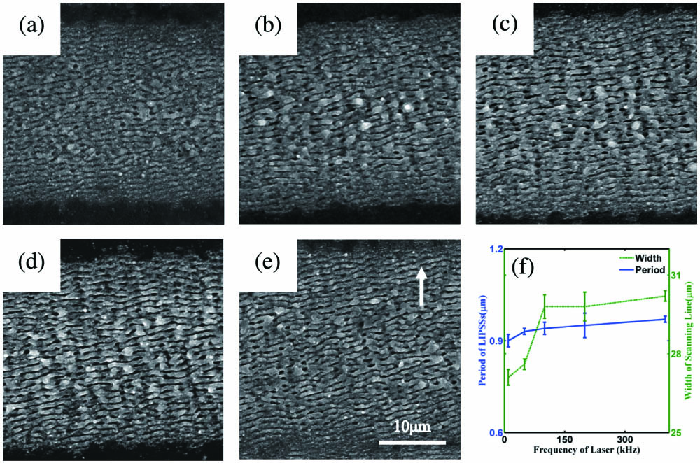
With a pulse overlapping rate of 91%, the influence of the repetition rate on surface morphology is shown in Figs. 1(a)–1(e). Figure 1(f) shows the ripple period and the scanning line width as a function of repetition rate. The resultant fringes are in the subwavelength scale, with period increasing from 0.9 to 0.97 µm when repetition rate is varied from 10 to 400 kHz; the subwavelength periodic pattern is rough at a low repetition rate, whereas it is intensively enhanced at a higher repetition rate; with growing repetition rate, the scanning line widens, and the sharp increase is at 100 kHz.
Sign up for Chinese Optics Letters TOC. Get the latest issue of Chinese Optics Letters delivered right to you!Sign up now
![]()
Figure 1.SEM images of subwavelength ripples induced by femtosecond laser pulses under repetition rates of (a) 10 kHz, (b) 50 kHz, (c) 100 kHz, (d) 200 kHz, and (e) 400 kHz at a pulse overlapping rate of 91%; (f) period of ripples and width of the scanning line as a function of repetition rate (SEM magnification, 2000; scale bar, 10 µm; white arrow, laser polarization).
During the laser irradiation, the laser energy is absorbed by free electrons due to the inverse bremsstrahlung. The absorption process is followed by thermalization within the electron subsystem, energy transfer from the electrons to the lattice, and heat transport into the target due to the electron thermal diffusion[22]. The lattice heating time is over a picosecond time scale. According to the numerical investigation of Chen et al., the lattice temperature at heat equilibrium is estimated to be 1000 K. Subsequently, the lattice follows a heat diffusion process[23],
![]()
Figure 2.(a) Surface temperature decay of silicon after a single pulse irradiation; calculated temperature as a function of time for repetition rates of (b) 10 kHz and (c) 400 kHz, respectively.
Morphological characteristics of subwavelength ripple structures induced by femtosecond laser pulses with pulse overlapping rates varying from 65% to 98% are illustrated in Figs. 3(a)–3(e). At a pulse overlapping rate of 65%, ripple structures emanate from a surface scratch denoted in the blue dashed circle [Fig. 3(a)]. The scratch is approximately 1 µm in length. Unlike the observed subwavelength structures in Fig. 1, the period of the cone-shaped fringes in this case is as long as the wavelength of the incident laser. A model of nonradiative “radiation remnants” can be responsible for the observed phenomenon, based on the assumption that the steady-state patterns result from inhomogeneous energy absorption just beneath the surface, induced by surface roughness[24,25]. When the pulse overlapping rate is increased to 83%, subwavelength periodic structures can not only be observed in the central area of the laser ablation region, but also begin to appear in the periphery area. We also note that the subwavelength ripple goes with a shorter period and deeper grooves in the periphery (marked by a red ellipse) [Fig. 3(b)]. In Fig. 3(f), it is evident that the ripple period becomes shorter with increased pulse overlapping rate. In addition, the repetition rate of 400 kHz induces a longer ripple period than that of 100 kHz at the same pulse overlapping rate.
![]()
Figure 3.SEM images of ripple structures induced by femtosecond laser pulses under pulse overlapping rates of (a) 65%, (b) 83%, (c) 91%, (d) 96%, and (e) 98% at a repetition rate of 400 kHz; (f) period of ripples as a function of the pulse overlapping rate at repetition rates of 10 and 400 kHz (SEM magnification, 3500; scale bar, 5 µm; white arrow, laser polarization).
The subwavelength surface ripples are considered to be due to SP–laser interference[20]. The propagating SPs and the incident laser interfere to form a fringe with a period written as
We estimated that substance above the air–silicon interface is air (), so the ripple period is simplified as
Increasing laser pulse irradiation gives rise to a higher lattice and electron temperature and therefore higher . For , with increasing , increases; thus, from Eq. (9), increases. This -increasing trend with growing temperature agrees well with observations in Fig. 1, where lengthens with increasing repetition rates, and in Fig. 3(f), where the repetition rate of 400 kHz results in a longer ripple period than that of 100 kHz. As described above, the ripple period in the periphery becomes shorter with deepened grooves [Fig. 3(b)]. This effect can be accounted for by the Gaussian distribution of the laser fields, where fluence in the periphery is much lower. Accordingly, by Eq. (9), lower periphery fluence means lower periphery , and therefore gives rise to shorter .
Huang et al. proposed that period-decreasing with increasing pulse overlapping rate is due to grating-assisted SP–laser coupling[20]. When the initial ripples are formed, deeper grooves make the laser field transfer to SPs more efficiently because of grating coupling effects. Hence, grooves grow as the number of pulses increases. As the groove deepens, the ripple period should decrease in order to satisfy the grating coupling condition. Based on this model, they also put forward an exceptional situation. When heat accumulation exists, a strong thermal effect will induce a thick melted layer and baffle the deepening of the groove. Accordingly, the grating coupling effect is weak, and the value of is mainly due to the interference mechanism and remains almost constant near as the pulse number increases.
However, in Fig. 3(f), it is evident that even at a repetition rate of 400 kHz where heat accumulation is quite strong, the ripple period still obeys an obvious decay trend with an increasing pulse overlapping rate. Therefore, we propose that the origin of the significantly reduced period with growing pulse overlapping rate is actually due to the Maxwell–Garnett effect[28]. During laser irradiation, the silicon surface was covered by extensive nanostructures. The femtosecond laser structured surface can be divided into two layers: a uniform LIPSS layer and an air–nanostructure composite layer. In this case, cannot be estimated to be 1 but should be replaced by the effective dielectric constant ( of the air–nanostructure composite). Therefore, is estimated using the Maxwell–Garnett theory[26],
Based on Eq. (9), we calculate and plot the as a function of [Fig. 4(a)]. As discussed above, increases with growing . The effective dielectric constant of the air–nanostructure composite () and SP wavelength () as functions of volume fraction of the silicon inclusion () are plotted in Fig. 4(b). With an increasing pulse overlapping rate, more nanostructures are generated, and is therefore strongly enhanced. We notice that continuously increases with . This increase in eventually reduces .
![]()
Figure 4.(a) SP wavelength as a function of electron density; (b) effective dielectric constant (εeff) of air–nanostructure composite on LIPSSs and SP wavelength as functions of volume fraction of the silicon inclusion.
Therefore, we can conclude that both the electron density and the volume fraction of the silicon inclusion are responsible for . In the formation of LIPSSs, the increasing pulse overlapping rate propels both the electron density and the volume fraction of the silicon inclusion to go up. However, higher electron density drifts toward longer, whereas increasing volume fraction drives toward shorter. The two mechanisms compete with each other. Finally, in our case, the volume fraction of the silicon inclusion plays a more important role, which agrees with our observations in Fig. 3(f). That is, is significantly reduced with the increasing pulse overlapping rate, whereas at a repetition rate of 400 kHz is slightly more enhanced than that at a repetition rate of 10 kHz. Moreover, the weak dependence of on repetition rates can also be observed in Fig. 1(f): exhibits a small increase from 0.9 to 0.97 µm when the repetition rate is varied from 10 to 400 kHz.
In addition, surface morphology under repetition rates of 10 and 400 kHz is compared. Figures 5(a)–5(c) are the LIPSSs under a repetition rate of 10 kHz, and Figs. 5(d)–5(f) are under 400 kHz. We can find that LIPSSs in Figs. 5(a)–5(c) are attached by micro- or nanoparticles, and therefore look somewhat obscure. In contrast, the repetition rate of 400 kHz produces more distinct and defined ripples. It is due to heat accumulation that lattice temperature is well above the melting point of silicon (1687 K) and more intense SPs are stimulated. The molten silicon is forced into periodic distribution by the high pressure of stimulated SPs. Once the lattice temperature relaxes, periodic distribution is solidified into periodic structures. The more intense the stimulated SPs are, the more regularly and tidily the silicon surface is engraved. So, in Figs. 1(a)–1(e), LIPSSs become more evident and neat with growing repetition rates.
![]()
Figure 5.Comparison of the surface morphology under (a)–(c) 10 kHz and (d)–(f) 400 kHz at pulse overlapping rates of (a), (d) 98%, (b), (e) 91%, and (c), (f) 83%, respectively (SEM magnification, 3500; scale bar, 5 µm; white arrow, laser polarization).
4. Conclusion
In conclusion, variable repetition rates between 10 and 400 kHz were used to study the relationship between heat accumulation and resulting periodic surface structures on silicon. It was found that when the repetition rate reached up to 100 kHz, heat accumulation became so evident that femtosecond laser micromachining could not be considered as a nonthermal process. Moreover, heat accumulation was shown to significantly enhance LIPSSs, which has not been previously recognized. The ripple morphology under higher repetition appeared more distinct and much neater as more intense SPs were stimulated, and accumulated heat gave rise to a molten silicon surface. Once the temperature relaxes, SP-induced periodic distribution on the silicon surface is solidified into periodic structures. The more intense the stimulated SPs are, the much better-defined and neater ripples are engraved on the silicon surface. In addition, the ripple period was confirmed to be accounted for by two competing factors: repetition rate and pulse overlapping rate. The ripple period drifted longer with a higher repetition rate, whereas it was significantly reduced by increasing the pulse overlapping rate. The increase in period with repetition rates is due to increased electron density. However, ripple period-decreasing trend with a growing pulse overlapping rate is proposed to be due to the volume fraction increase of the silicon inclusion in the air–nanostructure composite, based on the Maxwell–Garnett theory.
References

Set citation alerts for the article
Please enter your email address
© Copyright 2018-2021 | Chinese Laser Press. All Rights Reserved 沪ICP备15018463号-20