
Haitao Zhu, Renli Fu, Meng Fei, Caixia Wang, Lei Ji. Optical and Thermal Performance of LED Light Source Packaged by Al/Al2O3 Composite Substrate[J]. Acta Optica Sinica, 2017, 37(10): 1023002
- Acta Optica Sinica
- Vol. 37, Issue 10, 1023002 (2017)
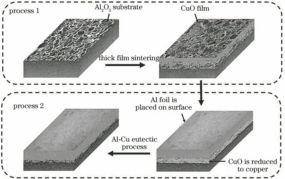
Fig. 1. Process of directing bonded aluminum on alumina substrate
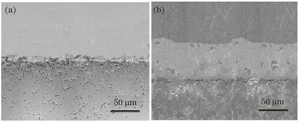
Fig. 2. Interface microstructure of Al/Al2O3 composite substrate. (a) Direct bonded aluminum; (b) soldering technology
Fig. 3. Peel strength of Al/Al2O3 composite ceramic substrate prepared by direct bonded aluminum and soldering technology
Fig. 4. 3D surface topography of Al/Al2O3 composite ceramic substrate disposed by different polishing methods. (a) Untreated; (b) chemical polishing; (c) electrolytic polishing; (d) chemical-mechanical polishing
Fig. 5. Surface roughness curves of Al/Al2O3 composite ceramic substrate disposed by different polishing methods. (a) Untreated; (b) chemical polishing; (c) electrolytic polishing; (d) chemical-mechanical polishing
Fig. 6. Reflective index of Al/Al2O3 composite ceramic substrate disposed by different polishing methods
Fig. 7. 3D optical model of round reflective cup. (a) Traditional Al2O3 ceramic substrate; (b) Al/Al2O3 ceramic substrate with high reflective index
Fig. 8. Schematic of hemispherical receiving surface model
Fig. 9. Simulation result of luminous efficiency of LED packaged by Al2O3 ceramic substrate. (a) Rectangular candela distribution plot; (b) polar iso-candela plot
Fig. 10. Simulation result of luminous efficiency of LED packaged by Al/Al2O3 composite substrate. (a) Rectangular candela distribution plot; (b) polar iso-candela plot
Fig. 11. Structure of Al/Al2O3 ceramic substrate prepared by two different technologies. (a) Soldering technology; (b) direct bonded aluminum
Fig. 12. Encapsulation heat dissipation model of Al/Al2O3 composite substrate
Fig. 13. Steady-state temperature distribution of encapsulation structure with different substrates under the thermal power of 4 W. (a) Direct bonded aluminum substrate; (b) soldering substrate
Fig. 14. Temperature difference of encapsulation structure with Al/Al2O3 ceramic substrate prepared by different preparation methods under different thermal power loads
Fig. 15. Sample packaged by Al/Al2O3 composite ceramic substrate
Fig. 16. Light intensity distribution and fitting curve of packaged LED source. (a) Normal Al2O3 ceramic substrate; (b) Al/Al2O3 composite ceramic substrate
Fig. 17. Schematic of homemade substrate heat conduction performance testing device
Fig. 18. Heat conduction performance of ceramic substrate prepared by different technologies. (a) Direct bonded aluminum; (b) soldering technology
|
Table 1. Relative parameters of each part of COB packaging model
|
Table 2. Size and relative thermal physical property parameters of Al/Al2O3 composite substrate

Set citation alerts for the article
Please enter your email address
© Copyright 2018-2021 | Chinese Laser Press. All Rights Reserved 沪ICP备15018463号-20