
Lijia Song, Tangnan Chen, Weixi Liu, Hongxuan Liu, Yingying Peng, Zejie Yu, Huan Li, Yaocheng Shi, Daoxin Dai, "Toward calibration-free Mach–Zehnder switches for next-generation silicon photonics," Photonics Res. 10, 793 (2022)
- Photonics Research
- Vol. 10, Issue 3, 793 (2022)
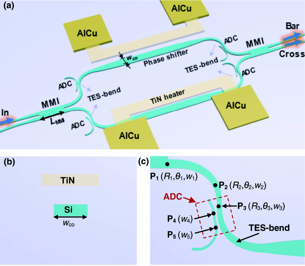
Fig. 1. Schematic configurations of the proposed calibration-free elementary 2 × 2
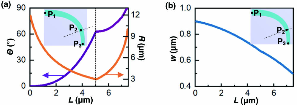
Fig. 2. (a) Local angle θ R w L
Fig. 3. Simulation results for the designed 2 × 2
Fig. 4. (a) Calculated total phase imbalance for the new MZS consisting of TES-bends as well as arm waveguides with different core widths of 1, 2, and 3 μm; here the mean width difference δ w w co
Fig. 5. (a) Optical microscope image of the fabricated 2 × 2 Q from 0 to 80 mW; (c) measured transmissions at the cross/bar ports of the present MZS operating at the Off/On (cross/bar) states (i.e., Q = 0
Fig. 6. (a) Optical microscope image, and (b)–(e) measured all-cross transmissions T i j O j I i i = 1 T i j I 1 I 2 I 3 I 4 O 1 O 2 O 3 O 4
Fig. 7. Synthesized eye-diagrams at port (a) O 1 O 2 O 3 4 × 4
Fig. 8. Adiabatic taper with different shapes. (a) Structure. (b) Calculated excess loss for the TE 0 TE 1 w co = 2 μm w 1 = 0.9 μm
Fig. 9. Simulated transmission spectra of the 2 × 2 TE 0 TE 1
Fig. 10. Calculated effective indices of the TE modes of 220-nm-thick silicon waveguides.
Fig. 11. (a), (b) Optical microscope images of TES-bend. (c) The measured transmissions for the testing structures with a number of TES-bends in cascade.
Fig. 12. Measured transmissions of the fabricated 4 × 4


Set citation alerts for the article
Please enter your email address

© Copyright 2018-2021 | Chinese Laser Press. All Rights Reserved 沪ICP备15018463号-20