Abstract
1. INTRODUCTION
Mach–Zehnder interferometers (MZIs) have been recognized as an indispensable fundamental element in various optical systems due to their great versatility for diverse applications [1–5]. In the past decades, on-chip MZIs have been developed with diverse material systems and have been widely used as one of the most essential components in photonic integrated circuits (PICs) [6–14]. Among them, silicon MZIs are becoming increasingly attractive because silicon photonics features ultrahigh integration density as well as excellent complementary metal-oxide semiconductor (CMOS) compatibility. Silicon MZIs have been developed successfully for realizing variable optical couplers [15,16], optical modulators [17], optical filters [18–21], variable optical attenuators [22], optical sensors [23], and optical switches [24–26]. Among them, Mach–Zehnder switches (MZSs) are one of the most representative functional elements and have been investigated for decades. In particular, thermo-optic (TO) MZSs feature excellent performances and design/fabrication simplicity [27–29], compared to their electro-optic (EO) counterparts based on carrier injection/depletion [24], and, hence, have been extensively investigated as a promising candidate for practical optical interconnects, such as optical burst switching (OBS) in the high-speed optical internet backbone.
Beyond a single MZS, it is also very important to achieve MZSs consisting of large-scale networks of MZSs in cascade. For example, and MZSs have been realized on silicon in recent years [30–32]. In this case, the total number of elementary MZSs scales up rapidly with the port count N, imposing increasingly stringent requirements on the performance of the elementary MZSs. A typical MZS is composed of two 3 dB couplers and two symmetric arms, designed for low excess losses and high extinction ratios. However, conventional MZSs are usually prone to the random size variations of the arm waveguides due to the imperfect fabrication with the state-of-the-art CMOS foundry processes, resulting in considerable accumulated random phase errors and unpredictable phase imbalance between the two arms. In this case, such random phase imbalance must be calibrated and compensated meticulously for all the MZSs one by one in a large-scale MZS. Therefore, a large number of additional power taps as well as power monitors are often required for all or part of the MZS elements, so that the optimal electrical power for their cross and bar states can be individually determined by monitoring the corresponding tapped power. However, this inevitably introduces significant excess losses. Furthermore, it also entails additional on-chip feedback control schemes and sophisticated characterization procedures, which significantly complicates the layout design and greatly increases the chip footprint as well as the chip management complexity. Besides, it also consumes extra heating power for both cross and bar states. Therefore, it becomes very challenging to scale up MZSs further. Recently, in Ref. [33], we proposed and demonstrated a new design of MZSs with lowered random phase errors for the first time by widening the straight phase-shifter waveguides, which effectively reduced the random phase imbalance, compared to the case of using conventional 0.45-μm-wide single-mode phase-shifters. The fabrication tolerance is, thus, improved, and the power consumption for compensating the phase imbalance is considerably reduced.
Here we propose a novel design toward calibration-free and MZSs that can be mass-manufactured in state-of-the-art silicon photonics foundries. The effective methodology to minimize the size variation sensitivity of the elementary MZS is to judiciously widen the entire MZI arm waveguides, including not only the straight phase-shifters but also the S-bends and the tapers, as well as the input/output waveguides of the multimode-interference (MMI) couplers. Specifically, the present MZS is designed and implemented by introducing novel tapered Euler S-bends (TES-bends) with a widened core width. Furthermore, bent asymmetric directional couplers (ADCs) are incorporated into the TES-bends to filter out residual higher-order modes at the TES-bend entrance. With a standard 180 nm CMOS foundry process, more than thirty MZSs with the proposed new design on 11 silicon photonic chips were fabricated and characterized. Compared with those conventional MZSs with 0.45-μm-wide single-mode phase-shifters, the present MZSs exhibit significant reduction in the random phase imbalance. This validates the improved fabrication tolerance and results in considerable reduction of the power consumption for the phase imbalance compensation. Furthermore, a MZS with Benes network topology is also fabricated with the same foundry process and characterized experimentally. The measured extinction ratios of the MZS and the MZS are 27–49 dB and across a broad wavelength range of , respectively, even without any calibrations. This work paves the way toward calibration-free large-scale silicon photonic MZSs. The proposed methodology for suppressing the random phase imbalance can be generalized for analog MZI elements and other essential phase-sensitive photonic integrated devices as well, such as micro-rings and arrayed-waveguide gratings (AWGs).
Sign up for Photonics Research TOC. Get the latest issue of Photonics Research delivered right to you!Sign up now
2. DESIGN OF THE ELEMENTARY
Figure 1(a) shows the schematic configuration of the proposed elementary MZS, which consists of two identical MMI couplers and two arm waveguides, and Fig. 1(b) shows the cross section of the phase-shifter with a TiN micro-heater on top. Each arm waveguide is composed of a phase-shifter, two adiabatic tapers, two TES-bends, and the straight sections connecting to the input/output ports of the MMI couplers. Here the MMI coupler is designed with a 2.4-μm-wide and 20.5-μm-long MMI section, while the width of the input/output waveguides for the MMI coupler is chosen as 0.9 μm. The TES-bends and the widened phase-shifters are connected through -long adiabatic tapers (see Appendix A, Fig. 8).
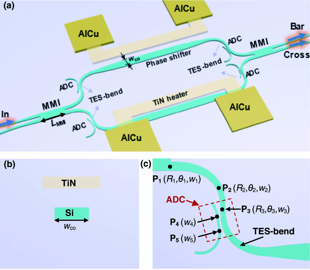
Figure 1.Schematic configurations of the proposed calibration-free elementary
The S-bends and the phase-shifters of conventional MZSs are usually single-mode, and, thus, their effective indices depend sensitively on the random variation of the core width due to the fabrication errors. Consequently, notable accumulated phase imbalance is usually observed between the two MZS arms due to the random difference in their core widths. A promising solution to this problem is to introduce widened phase-shifters, as proposed in our previous work [33], where the straight section in the phase-shifter is designed to be as wide as 2 μm. One might notice that the S-bends in the MZS arms in Ref. [33] are still as narrow as 450 nm to be single-mode, in order to avoid higher-order mode excitation. Such single-mode S-bends become the dominant contributor to the phase imbalance in the MZS arms.
In contrast, in this paper, it is the first time for incorporating specially designed multimode S-bends into MZSs, whose effective indices are much less dependent on the core width variation. As a result, the random phase imbalances can be greatly reduced. The challenge for such multimode S-bends in an MZS lies in the suppression of higher-order modes when light propagates in the arm waveguides. More specifically, the multimode S-bends should be designed with two key strategies to enable low-loss and low-cross-talk propagation of the fundamental mode. One is to quickly fan out the two waveguides connected with the MMI couplers to avoid any undesired evanescent coupling and thermal cross talk between them. The other is to filter out the residual higher-order modes, especially the dominant mode, which is slightly excited with a power ratio of due to imperfect self-imaging at the junction of the input MMI coupler (see Appendix A, Fig. 9). Furthermore, the S-bends should be as compact as possible to reduce the accumulated phase imbalance.
Here a special TES-bend with an incorporated bent-ADC mode filter is introduced, as shown in Fig. 1(c). The TES-bend consists of two identical 90° Euler-bends, whose curvature linearly decreases, with respect to the curve length , from at the end point (i.e., ) to at the knee point (i.e., ), and then linearly increases to at the deflection point (i.e., ), as shown in Fig. 2(a), where , , and are the respective curvature radii. Meanwhile, its width varies linearly with respect to the local angle , between the width at the end point , the width at the knee point , and the width at the deflection point , as shown in Fig. 2(b). Here the core width at the end point () is chosen as to match the MMI coupler input/output ports. Accordingly, the curvature radius is chosen as to simultaneously minimize the footprint and the mode mismatch between the MMI coupler input/output waveguides and the TES-bend. The core width and the bending radius at the deflection point () are chosen as and , respectively, so as to simultaneously minimize the footprint and the mode mismatch between those two sections with opposite curvatures. The other parameters at the knee points are optimally chosen as , , and . With this design, the footprint of the TES-bend is as small as .
Figure 2.(a) Local angle
Figure 3(a) shows the simulated light propagation in the designed TES-bend, where the propagation loss for the mode is negligibly low (less than 0.07 dB), while that for the mode is much higher (i.e., 1.97 dB) at 1550 nm. To further filter out the residual mode, a bent-ADC mode filter is incorporated into the second half of the TES-bend, without increasing the TES-bend footprint, as shown in Fig. 1(c). The bent-ADC mode filter consists of a coupling region where a narrow waveguide is introduced on the convex side near the deflection point of the TES-bend. There is a 0.2-μm-wide gap in the 1.3-μm-long coupling region, and the width of the narrow waveguide varies from 0.24 μm to 0.26 μm (see Appendix A, Fig. 10). In this way, the mode in the TES-bend can be coupled out to the mode in the narrow waveguide, leading to decent mode filtering within a highly compact footprint. Figure 3(b) shows the simulation results for light propagation of the and modes with the incorporation of the bent-ADC mode filter, which evidently suppresses the mode transmission by 12–17 dB, meanwhile introducing negligible transmission loss for the mode.
Figure 3.Simulation results for the designed
To further validate the TES-bend design, the simulated light propagation through the MMI coupler and the connected TES-bends is shown in Fig. 3(c). It exhibits excellent performances with low non-uniformity of , low excess loss of , and well-suppressed higher-order-mode excitation of in the wavelength range from 1520 nm to 1580 nm. When operating at the central wavelength of 1550 nm, the non-uniformity is about 0.06 dB, the excess loss is , and the higher-order mode excitation is . Finally, for the entire MZS consisting of the designed MMI couplers and TES-bends, the transmission spectra at the cross/bar ports are calculated with the finite-difference time-domain (FDTD) method, as shown in Fig. 3(d). It exhibits excellent performances with low excess losses of and high extinction ratios of in the wavelength range from 1520 nm to 1580 nm.
Figure 4(a) shows the calculated accumulated phase imbalance for the present MZS design as the mean width difference varies. In order to provide a quantitative comparison, the result for the conventional MZS is also given. As shown in Fig. 4(a), the designs with the present TES-bends as well as the widened phase-shifter with exhibit -fold lower phase imbalance than the conventional design with . Furthermore, the itemized phase imbalance [33] is analyzed theoretically and shown in Fig. 4(b). It can be seen that the present TES-bend has a lowered phase imbalance of 0.0064π/nm (gray solid line), which is -fold improvement over the conventional 450-nm-wide S-bend (purple dotted line), which is the most representative and widely employed [27,30,33,34]. Note that the TES-bend is still the dominant contributor to the total phase imbalance for the case with -wide phase-shifters.
Figure 4.(a) Calculated total phase imbalance for the new MZS consisting of TES-bends as well as arm waveguides with different core widths of 1, 2, and 3 μm; here the mean width difference
3. FABRICATION AND MEASUREMENT
Here the MZSs have been fabricated on silicon-on-insulator (SOI) wafers with a 220-nm-thick top silicon layer and a 2-μm-thick buried oxide (BOX) layer, using standard 180 nm CMOS foundry processes, as shown in Fig. 5(a). Here TiN micro-heaters are on top of both phase-shifters to balance the induced optical loss, if any. Grating couplers are used for convenient and efficient chip-fiber coupling. With the cut-back method, the excess loss of a single TES-bend (with the bent-ADC) has been separately measured to be as low as 0.068 dB [see Appendix A, Fig. 10(c)].
Figure 5.(a) Optical microscope image of the fabricated
Figures 5(b) and 5(c) show the measurement results for one of the representative MZSs with TES-bends and 2-μm-wide phase-shifters (Design A). From the measured transmissions at the cross/bar ports for the central wavelength when sweeping the heating power from 0 to 80 mW, shown in Fig. 5(b), the phase imbalance is very small, and the corresponding heating power for the compensation is only. The bar port has an extinction ratio as high as 32 dB even without any heating power (i.e., ) for phase imbalance compensation. From the transmission spectra at the cross/bar ports of the MZS operating in the Off/On (cross/bar) states (i.e., and 34 mW, respectively), the extinction ratios are 27–49 dB in the wavelength range from 1520 nm to 1580 nm. These results verify the excellent performance of the present MZS without any additional power consumption for the phase imbalance compensation, paving the way toward calibration-free MZSs.
To quantify the random phase imbalance for each MZS device, the cross and bar port transmissions at 1550 nm were measured by sweeping the heating power from 0 to 80 mW. From the measured transmission minima for the bar and cross ports, the heating powers and for the Off- and On-states can be determined, respectively, as shown in Fig. 5(b). Due to the random phase imbalance for each MZS, usually , as presented in our previous work [33], the TO phase shift is proportional to the heating power . Consequently, one has . In this way, the phase imbalance can be calculated from the measured and . Figure 5(d) provides the statistics for the calibrated phase imbalances for all the MZSs on our 11 chips diced from the same SOI wafer. There are four types of MZSs, including Design A described above, Design B with the TES-bends and 1-μm-wide phase-shifters, Design C with the conventional 0.45-μm-wide S-bends and 2-μm-wide phase-shifters, and Design D with the conventional 0.45-μm-wide S-bends/phase-shifters. As shown in Fig. 5(d), for Design D (i.e., the conventional design), the mean and standard deviation of the phase imbalance are and , respectively, denoted as for short in the following. Such large random phase imbalances must be calibrated and compensated carefully when the MZS is used. In contrast, when the phase-shifter is broadened to 2 μm, the random phase imbalance for Design C (with 0.45-μm S-bends and 2-μm-wide phase-shifters) is reduced greatly to be . When the S-bends are also broadened by introducing the TES-bend design, Design A (with TES-bends and 2-μm-wide phase-shifters) has a phase imbalance reduced further to , which indicates the phase imbalance can be reduced greatly by incorporating TES-bends into MZSs. For Designs B with the present TES-bends and 1-μm-wide phase-shifters, the phase imbalance is also very low, i.e., , as expected. The comparison between Designs A and B indicates that the random variation of the phase-shifters does not contribute dominantly to the phase imbalance when the core width is wider than 1 μm, consistent with the theoretical calculations in Fig. 4(b). As a summary, for Designs A and B, the superior performances with high extinction ratios and low excess losses are achieved even without any calibration for the Off state, as shown in Fig. 5(d). This promises to greatly simplify the calibration particularly for MZSs with a large number of MZSs, as well as to reduce the power consumption significantly for phase-imbalance compensation.
The present MZS with Design A is used further for the realization of a MZS with Benes network, which consists of six MZSs cascaded in three stages, as shown in Fig. 6(a). Here we only present the measured transmission spectra from the most representative switching states, i.e., all-cross, all-bar, and the six single-bar switching states (see Appendix A, Fig. 11). When the MZS operates in the all-cross state, the signals launched from input ports , , , and are routed to output ports , , , and , respectively. Figures 6(b)–6(e) show the measured all-cross transmission spectra at the output port from the input port when , 2, 3, and 4, respectively, with no calibration for any of the six MZSs (i.e., the powers applied to the six micro-heaters are zero). The extinction ratios for all the ports are across the 60 nm wavelength range. The extinction ratio for the MZS is lower than the MZS due to the accumulated cross talk of all the paths [35]. When the MZS operates in the all-bar state, the signals launched from input ports , , , and are routed to output ports , , , and , respectively. Figures 6(f)–6(i) show the measured all-bar transmission spectra defined above, exhibiting excellent performances similar to the cases with all-cross states.
Figure 6.(a) Optical microscope image, and (b)–(e) measured all-cross transmissions
The MZS is further used to demonstrate high-bit-rate data routing. In order to characterize the signal integrity degradation due to the MZS cross talk, eye-diagrams at any output port should be recorded when all four data channels are launched into the input ports (, 2, 3, and 4). However, due to the lack of concurrent data generators in the lab, we synthesize the eye-diagrams at the output port from the measured transmissions by reasonably assuming the four inputs are incoherent. In our experiments, the 30 Gb/s non-return-to-zero (NRZ) data were launched into the input ports one by one, and the transmissions from input port to output port were measured and recorded. The eye-diagram at the output port is synthesized by summing the transmissions (, 2, 3, and 4), i.e., . Figures 7(a)–7(d) show the synthesized eye-diagrams for ports , , , and , respectively, exhibiting open eye-diagrams with high signal-to-noise ratios, which validates the high-bit-rate data routing of the present MZS in the all-cross states.
Figure 7.Synthesized eye-diagrams at port (a)
4. CONCLUSION
Our theoretical analysis and experimental results above, especially the statistical comparison between our new MZS designs and the conventional one on the chips diced from the same SOI wafer, unambiguously confirm the effectiveness of our methodology to reduce the random phase imbalance. The present calibration-free Benes MZS already shows promising results that are sufficient for certain practical applications, which is an important first step toward large-scale calibration-free MZSs on silicon. More generally, excellent fabrication tolerance is an important premise that must be achieved to enable the further scaling of silicon photonic circuits, which is becoming the consensus of the silicon photonics community. We believe this work is an important breakthrough to meet the challenge of fabrication tolerance, which is currently a major hinderance for the real-world mass deployment of silicon photonic devices, especially the large-scale passive devices.
In conclusion, we have proposed a novel design toward calibration-free and MZSs that can be mass-manufactured in state-of-the-art silicon photonics foundries by judiciously widening the MZI arm waveguides. Specifically, the present MZS is designed and implemented by introducing novel TES-bends with a widened core width and incorporated bent-ADC mode filters. With a standard 180 nm CMOS foundry process, more than thirty MZSs and one Benes MZS with the new design have been fabricated and characterized. Compared with those conventional MZSs with 0.45-μm-wide single-mode phase-shifters, the present MZSs with 2-μm-wide phase-shifters exhibit a significantly suppressed random phase imbalance of . The fabricated and MZSs feature high extinction ratios of 27–49 dB and across a wavelength range, respectively, even without any calibrations. These results pave the way toward large-scale calibration-free silicon photonic MZSs while more effort should be made to prevent the extinction ratio from deteriorating due to the accumulated cross talk from all the paths. The proposed methodology for suppressing the random phase imbalance can be generalized for analog MZI elements and other essential phase-sensitive integrated photonic elements as well, such as micro-rings and AWGs. This is extremely attractive for developing next-generation silicon PICs with many elements as well as simplified calibrations.
Appendix A
In this work, we optimized the taper with compact nonlinear curves to achieve low excess loss and a widened core width to minimize the random phase error. For the 10-μm-long tapers considered here, different taper shapes have been introduced. The excess loss of the mode and the mode excitation ratio to the mode are calculated, and the corresponding results are shown in Fig.
Figure 8.Adiabatic taper with different shapes. (a) Structure. (b) Calculated excess loss for the
Figure 9.Simulated transmission spectra of the
Figure 10.Calculated effective indices of the TE modes of 220-nm-thick silicon waveguides.
Figure 11.(a), (b) Optical microscope images of TES-bend. (c) The measured transmissions for the testing structures with a number of TES-bends in cascade.
Figure 12.Measured transmissions of the fabricated
References
[1] Y. Li, L. Tong. Mach–Zehnder interferometers assembled with optical microfibers or nanofibers. Opt. Lett., 33, 303-305(2008).
[2] D. A. B. Miller. Perfect optics with imperfect components. Optica, 2, 747-750(2015).
[3] Y. Zhang, Q. Du, C. Wang, T. Fakhrul, S. Liu, L. Deng, D. Huang, P. Pintus, J. Bowers, C. A. Ross, J. Hu, L. Bi. Monolithic integration of broadband optical isolators for polarization-diverse silicon photonics. Optica, 6, 473-478(2019).
[4] S. Ghosh, S. Keyvaninia, Y. Shoji, W. Roy, T. Mizumoto, G. Roelkens, R. Baets. Compact Mach–Zehnder interferometer Ce:YIG/SOI optical isolators. IEEE Photon. Technol. Lett., 24, 1653-1656(2012).
[5] C. Zhang, P. Morton, J. Khurgin, J. Peters, J. Bowers. Ultralinear heterogeneously integrated ring-assisted Mach–Zehnder interferometer modulator on silicon. Optica, 3, 1483-1488(2016).
[6] A. M. Al-Hetar, A. B. Mohammad, A. S. M. Supaat, Z. A. Shamsan. MMI-MZI polymer thermo-optic switch with a high refractive index contrast. J. Lightwave Technol., 29, 171-178(2011).
[7] M. He, M. Xu, Y. Ren, J. Jian, Z. Ruan, Y. Xu, S. Gao, S. Sun, X. Wen, L. Zhou, L. Liu, C. Guo, H. Chen, S. Yu, L. Liu, X. Cai. High-performance hybrid silicon and lithium niobate Mach–Zehnder modulators for 100 Gbit s−1 and beyond. Nat. Photonics, 13, 359-364(2019).
[8] A. Ribeiro, A. Ruocco, L. Vanacker, W. Bogaerts. Demonstration of a 4 × 4-port universal linear circuit. Optica, 3, 1348-1357(2016).
[9] J. S. Barton, E. J. Skogen, M. L. Masanovic, S. P. Denbaars, L. A. Coldren. A widely tunable high-speed transmitter using an integrated SGDBR laser-semiconductor optical amplifier and Mach-Zehnder modulator. IEEE J. Sel. Top. Quantum Electron., 9, 1113-1117(2003).
[10] R. Amin, R. Maiti, Y. Gui, C. Suer, M. Miscuglio, E. Heidari, R. T. Chen, H. Dalir, V. J. Sorger. Sub-wavelength GHz-fast broadband ITO Mach–Zehnder modulator on silicon photonics. Optica, 7, 333-335(2020).
[11] H. Wang, H. Chai, Z. Lv, Z. Zhang, L. Meng, X. Yang, T. Yang. Silicon photonic transceivers for application in data centers. J. Semicond., 41, 101301(2020).
[12] P. Bhasker, J. Norman, J. Bowers, N. Dagli. Intensity and phase modulators at 1.55 μm in GaAs/AlGaAs layers directly grown on silicon. J. Lightwave Technol., 36, 4205-4210(2018).
[13] D. Korn, R. Palmer, H. Yu. Silicon-organic hybrid (SOH) IQ modulator using the linear electro-optic effect for transmitting 16QAM at 112 Gbit/s. Opt. Express, 21, 13219-13227(2013).
[14] X. Yang, M. S. Nisar, W. Yuan, F. Zheng, L. Lu, J. Chen, L. Zhou. Phase change material enabled 2 × 2 silicon nonvolatile optical switch. Opt. Lett., 46, 4224-4227(2021).
[15] W. R. Clements, P. C. Humphreys, B. J. Metcalf, W. S. Kolthammer, I. A. Walmsley. Optimal design for universal multiport interferometers. Optica, 3, 1460-1465(2016).
[16] M. Reck, A. Zeilinger, H. J. Bernstein, P. Bertani. Experimental realization of any discrete unitary operator. Phys. Rev. Lett., 73, 58-61(1994).
[17] A. Liu, R. Jones, L. Liao, D. Samara-Rubio, D. Rubin, O. Cohen, R. Nicolaescu, M. Paniccia. A high-speed silicon optical modulator based on a metal–oxide–semiconductor capacitor. Nature, 427, 615-618(2004).
[18] R. A. Soref, F. De Leonardis, V. M. N. Passaro. Reconfigurable optical-microwave filter banks using thermo-optically tuned Bragg Mach-Zehnder devices. Opt. Express, 26, 14879-14893(2018).
[19] F. Horst, W. M. J. Green, S. Assefa, S. M. Shank, Y. A. Vlasov, B. J. Offrein. Cascaded Mach-Zehnder wavelength filters in silicon photonics for low loss and flat pass-band WDM (de-)multiplexing. Opt. Express, 21, 11652-11658(2013).
[20] M. E. Ganbold, H. Nagai, Y. Mori, K. Suzuki, H. Matsuura, K. Tanizawa, K. Ikeda, S. Namiki, H. Kawashima, K. I. Sato. A large-scale optical circuit switch using fast wavelength-tunable and bandwidth-variable filters. IEEE Photon. Technol. Lett., 30, 1439-1442(2018).
[21] L. Shen, L. Lu, Z. Guo, L. Zhou, J. Chen. Silicon optical filters reconfigured from a 16 × 16 Benes switch matrix. Opt. Express, 27, 16945-16957(2019).
[22] Q. Wu, L. Zhou, X. Sun, H. Zhu, L. Lu, J. Chen. Silicon thermo-optic variable optical attenuators based on Mach–Zehnder interference structures. Opt. Commun., 341, 69-73(2015).
[23] K. Misiakos, I. Raptis, E. Makarona, A. Botsialas, A. Salapatas, P. Oikonomou, A. Psarouli, P. S. Petrou, S. E. Kakabakos, K. Tukkiniemi, M. Sopanen, G. Jobst. All-silicon monolithic Mach-Zehnder interferometer as a refractive index and bio-chemical sensor. Opt. Express, 22, 26803-26813(2014).
[24] M. Yang, W. M. J. Green, S. Assefa, J. Van Campenhout, B. G. Lee, C. V. Jahnes, F. E. Doany, C. L. Schow, J. A. Kash, Y. A. Vlasov. Non-blocking 4 × 4 electro-optic silicon switch for on-chip photonic networks. Opt. Express, 19, 47-54(2011).
[25] N. Dupuis, A. V. Rylyakov, C. L. Schow, D. M. Kuchta, C. W. Baks, J. S. Orcutt, D. M. Gill, W. M. J. Green, B. G. Lee. Ultralow crosstalk nanosecond-scale nested 2 × 2 Mach–Zehnder silicon photonic switch. Opt. Lett., 41, 3002-3005(2016).
[26] K. Suzuki, R. Konoike, G. Cong, K. Yamada, S. Namiki, H. Kawashima, K. Ikeda. Strictly non-blocking 8 × 8 silicon photonics switch operating in the O-band. J. Lightwave Technol., 39, 1096-1101(2021).
[27] S. Wang, D. Dai. Polarization-insensitive 2 × 2 thermo-optic Mach-Zehnder switch on silicon. Opt. Lett., 43, 2531-2534(2018).
[28] F. Duan, K. Chen, D. Chen, Y. Yu. Low-power and high-speed 2 × 2 thermo-optic MMI-MZI switch with suspended phase arms and heater-on-slab structure. Opt. Lett., 46, 234-237(2021).
[29] L. Chen, Y.-K. Chen. Compact, low-loss and low-power 8 × 8 broadband silicon optical switch. Opt. Express, 20, 18977-18985(2012).
[30] S. Zhao, L. Lu, L. Zhou, D. Li, Z. Guo, J. Chen. 16 × 16 silicon Mach–Zehnder interferometer switch actuated with waveguide microheaters. Photon. Res., 4, 202-207(2016).
[31] L. Qiao, W. Tang, T. Chu. 32 × 32 silicon electro-optic switch with built-in monitors and balanced-status units. Sci. Rep., 7, 42306(2017).
[32] K. Tanizawa, K. Suzuki, M. Toyama, M. Ohtsuka, N. Yokoyama, K. Matsumaro, M. Seki, K. Koshino, T. Sugaya, S. Suda, G. Cong, T. Kimura, K. Ikeda, S. Namiki, H. Kawashima. Ultra-compact 32 × 32 strictly-non-blocking Si-wire optical switch with fan-out LGA interposer. Opt. Express, 23, 17599-17606(2015).
[33] L. Song, H. Li, D. Dai. Mach–Zehnder silicon-photonic switch with low random phase errors. Opt. Lett., 46, 78-81(2021).
[34] K. Suzuki, G. Cong, K. Tanizawa, S.-H. Kim, K. Ikeda, S. Namiki, H. Kawashima. Ultra-high-extinction-ratio 2 × 2 silicon optical switch with variable splitter. Opt. Express, 23, 9086-9092(2015).
[35] N. Dupuis, B. G. Lee. Impact of topology on the scalability of Mach–Zehnder-based multistage silicon photonic switch networks. J. Lightwave Technol., 36, 763-772(2018).
Set citation alerts for the article
Please enter your email address