Starting from the groundbreaking work in graphene[1], the active research in two-dimensional (2D) layered materials has unveiled a number of exotic phenomena that are unique in the 2D limit. In addition to the semimetal graphene, the semiconducting transition metal dichalcogenides (TMDs) and the insulating hexagonal boron nitride (hBN) are also the main driving forces of the field. Specifically, since the discovery of single photon emitters (SPEs) in tungsten diselenide (WSe2) and hBN[2,3], layered materials have become a new playground for quantum optics and quantum photonics[4,5]. With the host being atomically thin, engineering the dielectric environment can effectively change the properties of SPEs in TMDs and hBN. Even more, one can dynamically tune the energies of SPEs by applying an external electric field or static strain. It is worth mentioning that these SPEs could also serve as local probes, which are extremely sensitive to the fluctuation of environment.
Although the field is rapidly evolving, the physical origin of SPEs in 2D layered materials is still a puzzle. It has been believed that the SPEs originate from defects, because sulfur and selenide vacancies are common in MoS2 and WSe2. In addition to the boron and nitrogen vacancies, theoretical calculations have also suggested antisite defects and substitutional defects with carbon or oxygen as the possible origin of SPEs in hBN[6]. As a result, the 2D community has considered that the origin of SPEs in layered materials should be similar to that of the nitrogen vacancy (NV) centers in diamond, where optically active defects emit single photons. However, the emission pattern in 2D layered materials is very different from that of the NV centers. Take hBN as an example. The emission energies of SPEs in hBN cover a wide range, with wavelength ranging from ~440 to ~800 nm, which suggests that defects alone could not explain the spectral variability. Another possible origin of the SPEs in layered materials is strain. On the one hand, it is hard to completely avoid strain in preparing atomically thin samples. On the other hand, several groups have shown that strain from nanopillars could introduce local bright spots which support single photon emission[7,8]. The successful demonstration of strain induced SPEs applies to both TMDs and hBN[9]. ‘Straintronics’ could also potentially support other layered materials to host SPEs.
But strain is not the main cause of SPEs in 2D materials. By directly correlating the SPEs with local strain using a combination of photoluminescence (PL), cathodoluminescence (CL) and nanobeam electron diffraction, Professor Dionne’s group in Standard University showed that several SPEs are observed without considerable strain[10]. This result indicates that strain is not solely responsible for the physical origin and the spectral variability. With the help of first-principles modelling, they found that at least four classes of defects are related to the SPEs emitting from 540 to 720 nm. These four possible color centers in hBN are the boron monovacancies (VB), its hydrogen and oxygen complexes, nitrogen monovacancies (VN) and CBVN, NBVN and O2BVN. To this point, it may be reasonable to speculate that strain and defect are both needed to the formation of SPE in layered materials.
In a recent paper that was published inNano Letters, Professor Zhang’s group from the Institute of Semiconductors came up with a new idea on the physical origin of SPEs[11]. According to their experimental observation and theoretical modelling, most SPEs in hBN originate from donor–acceptor pairs (DAP). The DAP transition is common among conventional semiconductors, such as silicon, diamond and GaN, and it describes a luminescence mechanism that involves the coulomb interaction between the ionized donors (D+) and acceptors (A–). Besides the charged sites, the light-induced electrons and holes can also be trapped by the neutral donor (D0) and acceptor (A0) before the radiative emission. Optical signature of DAP is generally characterized by a series of sharp emission lines at low temperatures.
DAP transition was recently predicted to exist in hBN[12], but no experimental evidence has been shown in this wide band gap layered material. In Tanet al.'s paper, the authors described that there are two types of DAP transitions in hBN: with donors and acceptors located at either the same (Type 1) or different (Type 2) atomic element sites. Considering the varying distances between the donors and acceptors, the two types of DAP transition are able to account for a number of emission lines ranging from ~1.6 to ~2.8 eV.
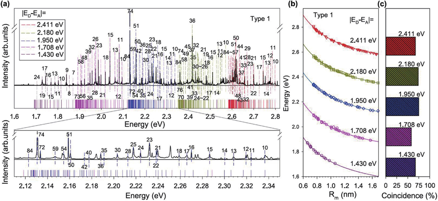
Fig. 1(a) shows a PL spectrum measured at 4 K, with sample prepared from the suspended hBN flakes in the 50/50 ethanol/water solution. The emission peaks, with linewidth down to ~75
eV, show a wide range of distribution in terms of energy from 1.544 to 2.800 eV. Tanet al. adopted the theoretical DAP model to calculate the emission lines and they found that approximately 70% of the emission peaks match well with the calculated DAP transition. The energy of the emission is described as follows:
![(Color online) (a) A PL spectrum taken at 4 K (solid line) with the calculated spectral distribution of type 1 DAPs shown in colored solid lines. (b) Calculated emission energies as a function ofRm, the distance between donors and acceptors. (c) Coincidence of measured emission energies. Figures are adapted from Ref. [11] with permission.](/Images/icon/loading.gif)
Figure 1.(Color online) (a) A PL spectrum taken at 4 K (solid line) with the calculated spectral distribution of type 1 DAPs shown in colored solid lines. (b) Calculated emission energies as a function ofRm, the distance between donors and acceptors. (c) Coincidence of measured emission energies. Figures are adapted from Ref. [11] with permission.
whereEA andED are the energy levels of the acceptor and donor.Rm represents them-th
nearest distance between the donors and acceptors, and this distance is determined by the crystal structure and lattice constant. The calculated energies of Type 1 DAP transitions with
being 2.411, 2.180, 1.950, 1.708, and 1.430 eV are shown in the colored lines fromFigs. 1(a) and1(b). With varying distances (Rm) between the donors and acceptors (Fig. 1(b)), the coulomb interaction
changes accordingly, and the emission energy could vary by ~200 meV for a fixed type of donor and acceptor (
). This reproduces the dense lines showing up inFig. 1(a). As shown in the coincidence plot fromFig. 1(c), the measured emission lines are in good agreement with the calculated results from the DAP models. For the emission lines that could not be explained by the DAP model, Professor Zhang’s group has suggested three possible explanations: (1) these SPEs originate from optically active defects without the DAP effects, (2) the energies of SPEs have shifted due to the presence of strain, and (3) inhomogeneous distribution of the defects.
This work from the Institute of Semiconductors has uncovered a new physical origin of SPEs in hBN. It also suggests a novel way to generate single photon emissions in other semiconductors, particularly those with efficient DAP transitions.
References
[1] K S Novoselov, A K Geim, S V Morozov et al. Electric field effect in atomically thin carbon films. Science, 306, 666(2004).
[2] M Toth, I Aharonovich. Single photon sources in atomically thin materials. Annu Rev Phys Chem, 70, 123(2019).
[3] X L Liu, M C Hersam. 2D materials for quantum information science. Nat Rev Mater, 4, 669(2019).
[4] M Turunen, M Brotons-Gisbert, Y Y Dai et al. Quantum photonics with layered 2D materials. Nat Rev Phys, 4, 219(2022).
[5] M Atatüre, D Englund, N Vamivakas et al. Material platforms for spin-based photonic quantum technologies. Nat Rev Mater, 3, 38(2018).
[6] S A Tawfik, S Ali, M Fronzi et al. First-principles investigation of quantum emission from hBN defects. Nanoscale, 9, 13575(2017).
[7] C Palacios-Berraquero, D M Kara, A R P Montblanch et al. Large-scale quantum-emitter arrays in atomically thin semiconductors. Nat Commun, 8, 15093(2017).
[8] A Branny, S Kumar, R Proux et al. Deterministic strain-induced arrays of quantum emitters in a two-dimensional semiconductor. Nat Commun, 8, 15053(2017).
[9] X H Xu, Z O Martin, D Sychev et al. Creating quantum emitters in hexagonal boron nitride deterministically on chip-compatible substrates. Nano Lett, 21, 8182(2021).
[10] F Hayee, L Yu, J L Zhang et al. Revealing multiple classes of stable quantum emitters in hexagonal boron nitride with correlated optical and electron microscopy. Nat Mater, 19, 534(2020).
[11] Q H Tan, J M Lai, X L Liu et al. Donor-acceptor pair quantum emitters in hexagonal boron nitride. Nano Lett, 22, 1331(2022).
[12] P Auburger, A Gali. Towardsab initio identification of paramagnetic substitutional carbon defects in hexagonal boron nitride acting as quantum bits. Phys Rev B, 104, 075410(2021).