• Photonics Research
  • Vol. 12, Issue 4, 854 (2024)
Yan-Hui Deng1, Yu-Wei Lu1、2, Hou-Jiao Zhang1, Zhong-Hong Shi1, Zhang-Kai Zhou1、3、*, and Xue-Hua Wang1、4、*
Author Affiliations
  • 1State Key Laboratory of Optoelectronic Materials and Technologies, School of Physics, Sun Yat-sen University, Guangzhou 510275, China
  • 2Quantum Science Center of Guangdong–Hong Kong–Macao Greater Bay Area (Guangdong), Shenzhen 518045, China
  • 3e-mail: zhouzhk@mail.sysu.edu.cn
  • 4e-mail: wangxueh@mail.sysu.edu.cn
  • show less
    DOI: 10.1364/PRJ.514576 Cite this Article Set citation alerts
    Yan-Hui Deng, Yu-Wei Lu, Hou-Jiao Zhang, Zhong-Hong Shi, Zhang-Kai Zhou, Xue-Hua Wang. Strong light–matter interactions based on excitons and the abnormal all-dielectric anapole mode with both large field enhancement and low loss[J]. Photonics Research, 2024, 12(4): 854 Copy Citation Text show less
    The fitted results. (a) Two-oscillator Fano fitting of the AAM of the SDR (green dashed line). The two individual oscillators are determined by curve fitting (blue solid line), and the red solid line represents the result of the numerical calculation. The SCS of (b) the SDR-WSe2 and (c) the SDR-J-agg fitted by a phenomenological coupled oscillator model. The black dashed lines represent the fitted results based on Eq. (5a), while the red solid lines represent the results of the numerical calculation.
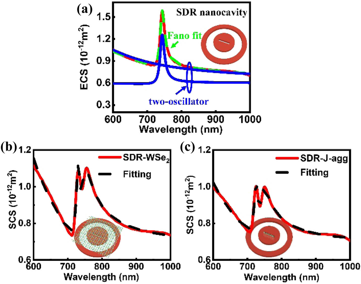
    Fig. 1. The fitted results. (a) Two-oscillator Fano fitting of the AAM of the SDR (green dashed line). The two individual oscillators are determined by curve fitting (blue solid line), and the red solid line represents the result of the numerical calculation. The SCS of (b) the SDR-WSe2 and (c) the SDR-J-agg fitted by a phenomenological coupled oscillator model. The black dashed lines represent the fitted results based on Eq. (5a), while the red solid lines represent the results of the numerical calculation.
    From a weak coupling system to a strong coupling system based on all-dielectric nanocavities. (a) Schematic diagrams of theoretical model for strong coupling. (b-i) and (b-ii) show the corresponding absorption and extinction cross sections (ACS, black line; ECS, red line) of the SD in (b-i) and the SDR in (b-ii). The schematic of different configurations is shown in the insets. The Fano fitting of the AAM of the SDR is represented in green dashed line. (c) The EF enhancements |E|/|E0| at the top surface (dashed lines) and center (solid lines) of the SD (black lines) and the SDR (red lines), respectively. The radius of the nanodisk is Rin=220 nm. The width and length of the slot are 10 and 260 nm. The inner and outer radii of the nanoring are Rin=390 nm and Rout=490 nm. Both nanodisk and nanoring have a height that is H=50 nm. The inset shows the minimum Nc to achieve strong coupling based on the SD and the SDR, and the right axis plots the ratio of gcSD/gcSDR. The calculation details of Nc are in Appendix B. (d) The scattering cross section (SCS) of the SD (blue line), the SD-WSe2 (green line), and the SD-J-agg (red line). (e) The SCS of the SDR, the SDR-WSe2, and the SDR-J-agg. The rigorous calculation results from FDTD were well fitted by a phenomenological coupled oscillator model (black dashed line). WSe2 and J-aggregates are placed on the top surface and center of the nanodisk, respectively. The linewidth of excitons is γex=50 meV for both the WSe2 monolayer and J-aggregates.
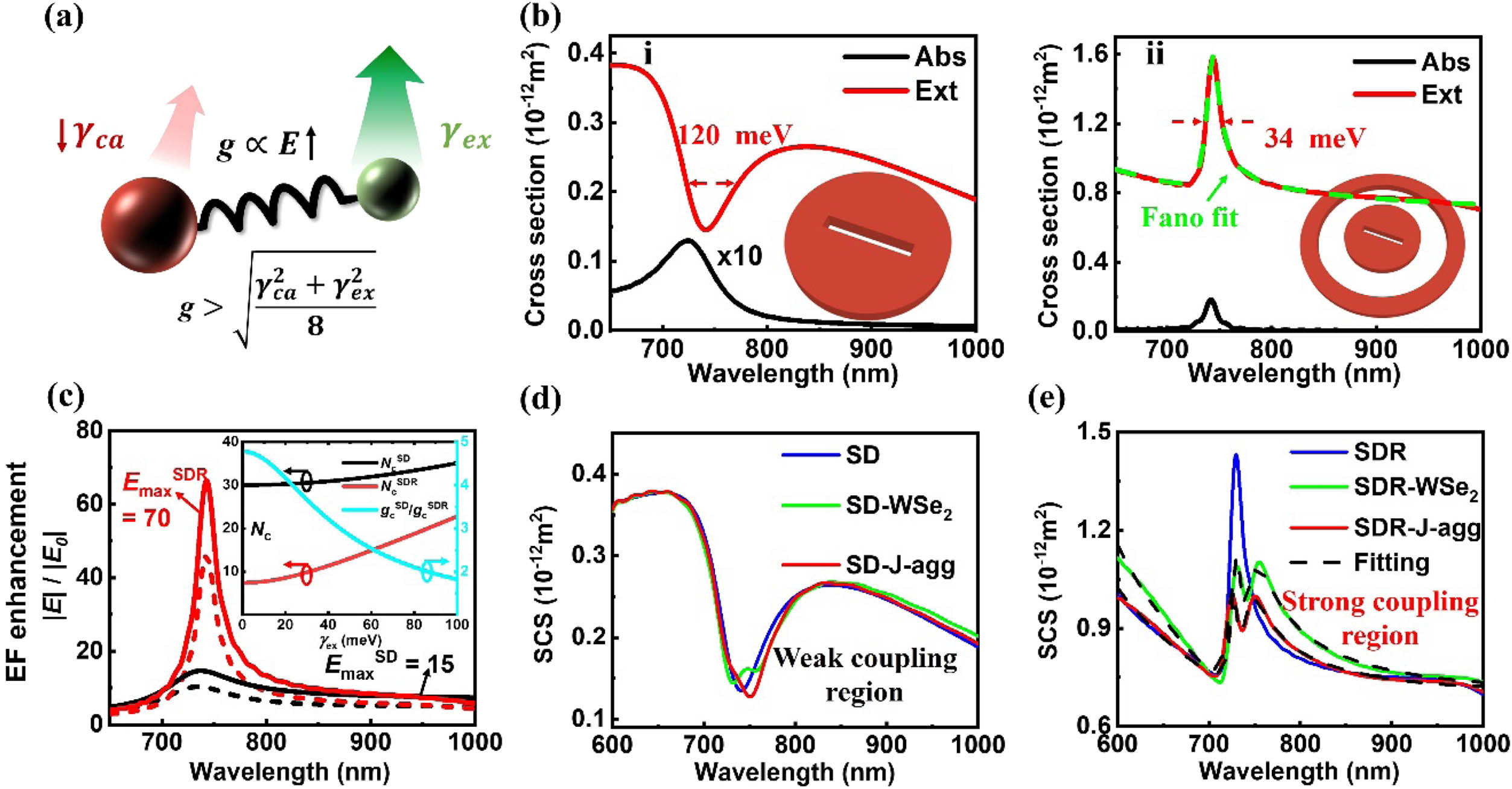
    Fig. 2. From a weak coupling system to a strong coupling system based on all-dielectric nanocavities. (a) Schematic diagrams of theoretical model for strong coupling. (b-i) and (b-ii) show the corresponding absorption and extinction cross sections (ACS, black line; ECS, red line) of the SD in (b-i) and the SDR in (b-ii). The schematic of different configurations is shown in the insets. The Fano fitting of the AAM of the SDR is represented in green dashed line. (c) The EF enhancements |E|/|E0| at the top surface (dashed lines) and center (solid lines) of the SD (black lines) and the SDR (red lines), respectively. The radius of the nanodisk is Rin=220  nm. The width and length of the slot are 10 and 260 nm. The inner and outer radii of the nanoring are Rin=390  nm and Rout=490  nm. Both nanodisk and nanoring have a height that is H=50  nm. The inset shows the minimum Nc to achieve strong coupling based on the SD and the SDR, and the right axis plots the ratio of gcSD/gcSDR. The calculation details of Nc are in Appendix B. (d) The scattering cross section (SCS) of the SD (blue line), the SD-WSe2 (green line), and the SD-J-agg (red line). (e) The SCS of the SDR, the SDR-WSe2, and the SDR-J-agg. The rigorous calculation results from FDTD were well fitted by a phenomenological coupled oscillator model (black dashed line). WSe2 and J-aggregates are placed on the top surface and center of the nanodisk, respectively. The linewidth of excitons is γex=50  meV for both the WSe2 monolayer and J-aggregates.
    Optical responses of individual Si SD and Si SDR nanocavities. (a) The contributions from different expansion multipole modes to the scattering spectrum of the SD. They are ED, MD, EQ, MQ, and Sum (blue, pink, olive, cyan, and black solid lines) as well as the simulation calculation (FDTD, red dashed line). The MD contribution approaches 0, and it is covered by the olive line. The inset shows the contribution of MD and EQ. (b) Charge distribution in the SD excited by normal incidence plane wave with polarization along the y axis. The red arrow in the diagram shows the direction where the charge is moving. (c) The resonant near-field profiles on the z=0 nm (center of the slot), z=25 nm (top surface of the SD), x=0 nm, and y=0 nm planes of the SD. (d)–(f) The same contents of the SDR as that in (a)–(c), respectively. The black circles and white lines show the outlines and boundaries of the nanostructures. The origin of the coordinate system is placed at the center of the disk.
    Fig. 3. Optical responses of individual Si SD and Si SDR nanocavities. (a) The contributions from different expansion multipole modes to the scattering spectrum of the SD. They are ED, MD, EQ, MQ, and Sum (blue, pink, olive, cyan, and black solid lines) as well as the simulation calculation (FDTD, red dashed line). The MD contribution approaches 0, and it is covered by the olive line. The inset shows the contribution of MD and EQ. (b) Charge distribution in the SD excited by normal incidence plane wave with polarization along the y axis. The red arrow in the diagram shows the direction where the charge is moving. (c) The resonant near-field profiles on the z=0  nm (center of the slot), z=25  nm (top surface of the SD), x=0  nm, and y=0  nm planes of the SD. (d)–(f) The same contents of the SDR as that in (a)–(c), respectively. The black circles and white lines show the outlines and boundaries of the nanostructures. The origin of the coordinate system is placed at the center of the disk.
    Cartesian multipole decomposition results of the SCS for the SDR nanocavity including the original electric dipole (P, black solid line) mode, toroidal dipole (T, red solid line) mode, and ED (blue dashed line) mode. When P and T have the same amplitude and opposite phase (i.e., P=−ikT) [47], there is the destructive interference between P and T, resulting in the anapole mode (AM).
    Fig. 4. Cartesian multipole decomposition results of the SCS for the SDR nanocavity including the original electric dipole (P, black solid line) mode, toroidal dipole (T, red solid line) mode, and ED (blue dashed line) mode. When P and T have the same amplitude and opposite phase (i.e., P=ikT) [47], there is the destructive interference between P and T, resulting in the anapole mode (AM).
    SCS of the SDR by varying (a) the refractive index n from 3.4 to 6.0 and (c) the height H from 30 to 100 nm, respectively. (b) and (d) The corresponding EF enhancements at the center of the slot. The other parameters are the same as those in Fig. 2.
    Fig. 5. SCS of the SDR by varying (a) the refractive index n from 3.4 to 6.0 and (c) the height H from 30 to 100 nm, respectively. (b) and (d) The corresponding EF enhancements at the center of the slot. The other parameters are the same as those in Fig. 2.
    Strong coupling behaviors of the Si SDR-exciton hybrid system. (a) Simulation model. For Type 1, the excitons are considered as a WSe2 monolayer of 1 nm covered on the top and bottom surfaces of the SDR. For Type 2, the J-aggregates (its sizes are Lx=120 nm, Ly =10 nm, and Lz) are placed in center of the slot. (b), (c) Optical energy diagrams of the SDR by manipulating the radii (b) RD and (c) Rs of the nanodisk and nanoring, where the black dashed lines denote the λAAM. The radius of the nanoring (Rs=Rout−Rin2) is tuned, while the Rout−Rin is fixed at 100 nm for all the rings. (d) Energy dispersions (Type 1, top; Type 2, bottom) of the hybrid states extracted from the simulations [blue dot, upper polariton branch (UP); red dot, lower polariton branch (LP)] and fitted using Eq. (7a) in Appendix B (solid curves). (e) The scattering spectra of Type 2 by varying the thickness Lz of the J-aggregates.
    Fig. 6. Strong coupling behaviors of the Si SDR-exciton hybrid system. (a) Simulation model. For Type 1, the excitons are considered as a WSe2 monolayer of 1 nm covered on the top and bottom surfaces of the SDR. For Type 2, the J-aggregates (its sizes are Lx=120  nm, Ly=10  nm, and Lz) are placed in center of the slot. (b), (c) Optical energy diagrams of the SDR by manipulating the radii (b) RD and (c) Rs of the nanodisk and nanoring, where the black dashed lines denote the λAAM. The radius of the nanoring (Rs=RoutRin2) is tuned, while the RoutRin is fixed at 100 nm for all the rings. (d) Energy dispersions (Type 1, top; Type 2, bottom) of the hybrid states extracted from the simulations [blue dot, upper polariton branch (UP); red dot, lower polariton branch (LP)] and fitted using Eq. (7a) in Appendix B (solid curves). (e) The scattering spectra of Type 2 by varying the thickness Lz of the J-aggregates.
    Strong coupling behavior and lasing action of the Si SDR-exciton on substrate. (a) The SCS of three hybrid systems: system I (SDR on substrate), system II, and system III (SDR-WSe2 on substrate), respectively. The width of the slot is changed to 30 nm when other parameters are the same as those in Fig. 2(b-ii). (b) Optical energy diagram of system III by manipulating the RD. (c) The SCS of the SDR-J-agg on substrate by varying the Lz of J-aggregates (γex=50 meV). (d) Optical energy diagram of the SDR-J-agg on substrate by manipulating the RD, where the Lz=8 nm. The insets schematically show the geometries of the different hybrid systems. (e) Lasing threshold of SD-QE (navy line) and SDR-QE (red line) versus the QE number. The solid and dashed lines represent structures on SDsub, SDRsub and without a substrate, respectively. The light green area indicates the parameter range where the SDRsub can lase while the SDsub cannot. (f) The corresponding lasing action of SDsub (top panel) and SDRsub (bottom panel) with 2000 QEs and a pump rate of P=20γ0, where γ0 is the spontaneous emission rate of QE. The dipole moment of QEs is 20 Debye, and the linewidth is γex=35 meV [11].
    Fig. 7. Strong coupling behavior and lasing action of the Si SDR-exciton on substrate. (a) The SCS of three hybrid systems: system I (SDR on substrate), system II, and system III (SDR-WSe2 on substrate), respectively. The width of the slot is changed to 30 nm when other parameters are the same as those in Fig. 2(b-ii). (b) Optical energy diagram of system III by manipulating the RD. (c) The SCS of the SDR-J-agg on substrate by varying the Lz of J-aggregates (γex=50  meV). (d) Optical energy diagram of the SDR-J-agg on substrate by manipulating the RD, where the Lz=8  nm. The insets schematically show the geometries of the different hybrid systems. (e) Lasing threshold of SD-QE (navy line) and SDR-QE (red line) versus the QE number. The solid and dashed lines represent structures on SDsub, SDRsub and without a substrate, respectively. The light green area indicates the parameter range where the SDRsub can lase while the SDsub cannot. (f) The corresponding lasing action of SDsub (top panel) and SDRsub (bottom panel) with 2000 QEs and a pump rate of P=20γ0, where γ0 is the spontaneous emission rate of QE. The dipole moment of QEs is 20 Debye, and the linewidth is γex=35  meV [11].
    The numerical and fitted results of the Purcell factor for the SD (navy solid line) and the SDR (red solid line) at z=0 nm. The fitted results of the Purcell factor (green dashed lines). (a) and (b) represent structures without SD, SDR and on substrate SDsub, SDRsub, respectively. This comparison shows good agreement.
    Fig. 8. The numerical and fitted results of the Purcell factor for the SD (navy solid line) and the SDR (red solid line) at z=0  nm. The fitted results of the Purcell factor (green dashed lines). (a) and (b) represent structures without SD, SDR and on substrate SDsub, SDRsub, respectively. This comparison shows good agreement.
    Yan-Hui Deng, Yu-Wei Lu, Hou-Jiao Zhang, Zhong-Hong Shi, Zhang-Kai Zhou, Xue-Hua Wang. Strong light–matter interactions based on excitons and the abnormal all-dielectric anapole mode with both large field enhancement and low loss[J]. Photonics Research, 2024, 12(4): 854
    Download Citation