Yan-Hui Deng, Yu-Wei Lu, Hou-Jiao Zhang, Zhong-Hong Shi, Zhang-Kai Zhou, Xue-Hua Wang, "Strong light–matter interactions based on excitons and the abnormal all-dielectric anapole mode with both large field enhancement and low loss," Photonics Res. 12, 854 (2024)
Copy Citation Text
【AIGC One Sentence Reading】:We propose an abnormal anapole mode that offers a strong electric field enhancement with low loss, significantly reducing the lasing threshold and paving the way for efficient on-chip nanophotonic devices.
【AIGC Short Abstract】:This study introduces the abnormal anapole mode, which offers a unique combination of strong electric field enhancement and low loss. This mode could significantly reduce the lasing threshold of quantum emitters, marking a crucial advancement for the on-chip integration of nanophotonic devices and opening new possibilities in fundamental and applied physics.
Note: This section is automatically generated by AI . The website and platform operators shall not be liable for any commercial or legal consequences arising from your use of AI generated content on this website. Please be aware of this.
Abstract
The room temperature strong coupling between the photonic modes of micro/nanocavities and quantum emitters (QEs) can bring about promising advantages for fundamental and applied physics. Improving the electric fields (EFs) by using plasmonic modes and reducing their losses by applying dielectric nanocavities are widely employed approaches to achieve room temperature strong coupling. However, ideal photonic modes with both large EFs and low loss have been lacking. Herein, we propose the abnormal anapole mode (AAM), showing both a strong EF enhancement of -fold (comparable to plasmonic modes) and a low loss of 34 meV, which is much smaller than previous records of isolated all-dielectric nanocavities. Besides realizing strong coupling, we further show that by replacing the normal anapole mode with the AAM, the lasing threshold of the AAM-coupled QEs can be reduced by one order of magnitude, implying a vital step toward on-chip integration of nanophotonic devices.
1. INTRODUCTION
The strong coupling system between the photonic modes of micro/nanocavities and quantum emitters (QEs; i.e., molecular excitons, quantum dots, and color centers) is a resultful way to construct room temperature quantum states that can be used to form controllable quantum bits with valuable applications in extensible solid quantum devices and chips [1–3]. Therefore, in the past decades, the studies of strong coupling have demonstrated advances varying from fundamental physics to integrated optoelectronics, quantum computing, and even quantum chemistry [4], giving rise to applications such as near-unity absorption [5], superconducting qubits [6], and controllable chemical reactions [7].
Generally, improving the electric field (EF) enhancements [8–10] and reducing the loss of photonic modes [11] are two vital ways to achieve strong coupling. So, plasmonic nanocavities have made great progress in the study of the strong coupling, due to their natural advantages of intensively strong EF enhancements. For example, not only has room temperature strong coupling based on surface lattice resonances or propagating surface plasmon been observed in many nanoarrays [12], but visible Rabi splitting has also been achieved in metal nanoparticle dimers [13]. Even the strong coupling at single exciton level by increasing the coupling strength has been demonstrated in various plasmonic systems [14], including the single nanorod [8,9], nanoparticle-on-mirror [15], and plasmonic bowtie [13].
On the other hand, all-dielectric nanostructures with a high-refractive index have been widely used in the study of cavity quantum electrodynamics [16] in recent years due to their abundant electromagnetic modes and low optical loss [17], such as nanospheres [18] and nanodisks [10,19]. In particular, the anapole mode (AM) in dielectric nanocavities has received widespread attention due to the suppressed far field and enhanced near field caused by nonradiative resonance behavior [20–22]. The all-dielectric nanocavities have negligible ohmic losses, strong electromagnetic resonances, and higher damage thresholds, enabling many novel functionalities such as nonlinear and quantum regimes, which are regarded as being able to pave the way for nonlinear devices, quantum-entangled light sources, and optical sensors [17]. There are good results on the strong coupling achieved by quasi-bound states in the continuum based on periodic photonic structures [23–25], but it is still challenging to obtain individual all-dielectric nanocavities with small loss, as well as large EF enhancements comparable to plasmonic cavities.
Sign up for Photonics Research TOC. Get the latest issue of Photonics Research delivered right to you!Sign up now
To this end, we propose the silicon (Si) slotted disk-ring (SDR) nanocavity with the abnormal anapole mode (AAM) to construct a strong coupling system. To the best of our knowledge, the AAM is a novel optical mode originating from the hybridization of AM and magnetic quadrupole (MQ) mode. Therefore, the AAM has a typical near-field distribution similar to AM, which exhibits two closed-loop currents with opposite directions along the torus, and a highly curved magnetic loop leading to energy confinement inside the nanodisk [26–28]. On the other side, due to the coherent coupling between the MQ mode and AM, the AAM exhibits a radiative peak with a narrower linewidth in the scattering spectrum, which is different from the nonradiative dip of AM. Compared to previous studies, it is found the AAM not only demonstrates an almost minimal loss in individual all-dielectric systems, but also supports EF enhancements comparable to most plasmonic nanocavities. Therefore, based on the AAM, the SDR-QE system can enter the strong coupling region with fewer excitons within a 10–1000 times smaller interaction region than those of previous works with all-dielectric systems. Furthermore, the lasing actions of the coupled systems of QEs and AAM (or AM) have also been theoretically investigated. Due to the advantages of AAM, the lasing threshold and output power of the SDR-QE system are, respectively, one order of magnitude lower and higher than those of the slotted disk-QE (SD-QE) system. Our findings not only contribute to the understanding of the enhanced light–matter interaction, but also help provide a promising platform for future nanophotonic applications such as nanolasers [29,30] and information processing [31].
2. PRINCIPLES AND METHODS
A. Numerical Simulation
Numerical calculations are conducted using Lumerical FDTD solutions. A total-field scattered-field (TFSF) plane wave serves as the excitation source. The excitation source is a normally incident plane wave polarized along the axis (the short side of the slot), and the origin of the coordinate system coincides with the center of the nanodisk. To simulate the nanostructure placed in an infinite space, perfectly matched layer (PML) boundary conditions are used. In our simulation, the Si nanodisk has an air slot with a width () of 10 nm and a length of 260 nm. The inner and outer radii of the nanoring are nm and , respectively. The height of nanodisk and nanoring is 50 nm. The dielectric constants of the Si are taken from Palik’s book. The surrounding index is for simulations. The mesh size is for the region around the structures, while the mesh size is and around the slot region and the monolayer.
B. Two-Oscillator Fano-Like Model
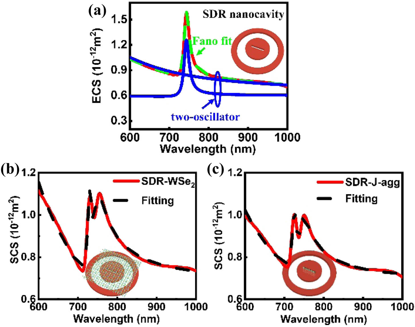
The extinction spectrum of the abnormal anapole mode (AAM) can be fitted by employing a Fano-like line shape [i.e., ] [32] to get where is the background amplitude, , , , and are the amplitude, damping, phase, and resonant energy of the oscillator in the resonant state. A two-oscillator (, 2) model is employed to fit the extinction spectrum, and a consistency was obtained for the calculated and fitted spectra, as shown in Fig. 1(a). The Fano-like line shape of AAM is caused by the coupling of the ED and MQ modes.
Figure 1.The fitted results. (a) Two-oscillator Fano fitting of the AAM of the SDR (green dashed line). The two individual oscillators are determined by curve fitting (blue solid line), and the red solid line represents the result of the numerical calculation. The SCS of (b) the and (c) the SDR-J-agg fitted by a phenomenological coupled oscillator model. The black dashed lines represent the fitted results based on Eq. (5a), while the red solid lines represent the results of the numerical calculation.
The optical response of the exciton is described, using a classical one-oscillator Lorentzian model, as where denotes the high-frequency component of the dielectric function of the exciton, and are transition frequency and linewidth of the exciton, and is the oscillator strength, which is proportional to the thickness of the two-dimensional material or the concentration of molecules. We use excitons from two kinds of materials: and J-aggregates. According to the experimental reports of [33,34] and J-aggregates [16,35], the parameters of these two excitons were artificially unified and set to , , , and .
D. Fitting with a Classical Coupled-Oscillator Model
The coupled oscillator model is a phenomenological model that describes the coupling between resonators and excitons [36,37]. For the SDR-exciton system, a harmonic oscillator is used to describe the resonance of the excitons and the dielectric cavity. Here, the dielectric cavity is described as two harmonic oscillators (cavity 1 and cavity 2) whose resonant frequencies are far apart. Furthermore, the interaction between the dielectric cavity and excitons is actually the near-field interaction of three harmonic oscillators, which can be characterized by the coupling strength of and . Due to the resonant frequency of cavity 2 being far from the transition frequency of excitons, which leads to , we also ignore the interaction between cavity 1 (ca1) and cavity 2 (ca2). Then, the motion equations of three oscillators can be written as where , , and represent the coordinates of the dielectric cavity and the exciton oscillations, and represents the external force. The , , and represent the damping rates of the dielectric cavity and the excitons. The , , and represent the resonance frequency of the excitons. and represent the coupling strength between the two harmonic oscillators describing the dielectric cavity and the excitons, respectively.
When the frequency of incident light is , the driving force is . At a steady state, , , and can be obtained based on frequency as
In a quasi-static approximation, the polarizability of the nanostructures is introduced and given as . Here, the contribution of the excitons to the total scattering field is negligible. Thus, the scattering cross-section (SCS) of the coupled system can be obtained by solving [37] where the wavevector , and . Substituting the expression to Eq. (4d), we can obtain the SCS as with the scattering amplitude A [38]. The fitted results of the SCS based on Eq. (5a) are shown in Figs. 1(b) and 1(c). For and SDR-J-aggregates (SDR-J-agg) heterostructures, the coupling strengths are fitted as (), 29 meV (SDR-J-agg), and . One can find that the fitted results based on the coupled-oscillator model match better with the results of the numerical calculation. Here, due to the influence of the background refractive index of the excitons, the resonant wavelength of the nanocavity will slightly redshift. Notably, if the contribution of excitons is large enough, the scattering cross section should be accurately written as
3. RESULTS AND DISCUSSION
The condition for strong coupling is that the coupling strength between the photonic mode and resonant excitons can overcome their respective damping decays and form an energy exchange between them [33,36]. Since the coupling strength is proportional to the localized EF enhancements, to get the to overpass the system losses of [including and , indicating the linewidths of the cavity and excitons, as shown in Fig. 2(a)], there are generally two ways available: one is to improve the EF and another is to reduce the loss [11]. Following these two ideas, we present the AAM and start our investigation by demonstrating its larger EF enhancements and smaller system loss, when compared to the normal AM or other photonic modes in all-dielectric systems.
Figure 2.From a weak coupling system to a strong coupling system based on all-dielectric nanocavities. (a) Schematic diagrams of theoretical model for strong coupling. (b-i) and (b-ii) show the corresponding absorption and extinction cross sections (ACS, black line; ECS, red line) of the SD in (b-i) and the SDR in (b-ii). The schematic of different configurations is shown in the insets. The Fano fitting of the AAM of the SDR is represented in green dashed line. (c) The EF enhancements at the top surface (dashed lines) and center (solid lines) of the SD (black lines) and the SDR (red lines), respectively. The radius of the nanodisk is . The width and length of the slot are 10 and 260 nm. The inner and outer radii of the nanoring are and . Both nanodisk and nanoring have a height that is . The inset shows the minimum to achieve strong coupling based on the SD and the SDR, and the right axis plots the ratio of . The calculation details of are in Appendix B. (d) The scattering cross section (SCS) of the SD (blue line), the (green line), and the SD-J-agg (red line). (e) The SCS of the SDR, the , and the SDR-J-agg. The rigorous calculation results from FDTD were well fitted by a phenomenological coupled oscillator model (black dashed line). and J-aggregates are placed on the top surface and center of the nanodisk, respectively. The linewidth of excitons is for both the monolayer and J-aggregates.
As shown in Figs. 2(b-i) and 2(c), for a normal AM (i.e., the SD nanocavity), the loss is 120 meV, while the maximal EF enhancements (black lines) at different locations can range from 11 (surface) to 15 (center). On the other hand, for our proposed AAM generated in the SDR nanocavity [Fig. 2(b-ii) and Fig. 2(c)], due to the constructive coherence between the AM and the MQ mode, its loss can be reduced to 34 meV (see Fig. 1 for the Fano fitting), together with its at different locations ranging from 45 (surface) to 70 (center, red solid line). It is noteworthy that the EF enhancements of 45–70 are comparable to plasmonic systems, such as the nanoarray with a lattice mode [39], the dimer with a localized plasmon mode [40], and the open cavity with a surface plasmon mode [8].
The low loss and large EF enhancements of AAM are greatly beneficial for its strong coupling with excitons, especially to meet the harsh strong coupling criterion in the emission spectrum (i.e., ). Note that it can be named the emission strong coupling condition (i.e., the ESC condition in Appendix A) [11,41]. As shown in the inset of Fig. 2(c), the critical coupling strength for multi-exciton strong coupling reduces from to for an exciton with a 20 Debye dipole moment and a linewidth at room temperature [11,42], which means the minimum (i.e., the number of excitons involved in a strong coupling interaction) that meets the requirement of can be reduced from to (see Appendix B).
The advantage becomes more obvious with a reduced exciton linewidth, which creates favorable conditions for lowering the required to achieve strong coupling. As a result, when we compare it to the normal AM generated by the SD, we find that when the involved is the same, it is impossible, using the normal AM, to achieve strong coupling effects [Fig. 2(d)]; however, applying AAM will be successful. According to the results shown in Fig. 2(e), the interaction between the SDR and excitons has reached the strong coupling region based on the criterion of both spectral splitting and energy level splitting (see Appendix A) [41,43]. In Figs. 2(d) and 2(e), the monolayer (1 nm) is on the top surface of the SDR or SD, and the J-aggregates are filled in the slot with a three-dimensional size of , , and . To fit the asymmetry spectral profiles in our systems, as well as to precisely obtain the system loss and coupling strength, a two-oscillator Fano-like model and the coupled oscillators model [32,36–38] are introduced to simulate and analyze the strong coupling system.
In fact, it is difficult to generate large EF enhancements and small loss simultaneously in optical nanocavities. The reported AM has only achieved great EF enhancements, and it still suffers from high loss [44]. To explain the advantages of the AAM (i.e., a large EF and small loss), we conducted a more in-depth numerical simulation and analysis.
As shown in Fig. 3, the optical responses of the SD and SDR, including multipole decompositions of the SCS, charge distributions, and near-field enhancements at the resonant wavelength of AM or AAM ( or ), are investigated. Through comparative analysis, it can be intuitively found that no matter the far-field response or near-field effect, the SDR nanocavity has overwhelming advantages such as large EF and low loss. The subtle deviation between the sum of multipole contributions (Sum, black) and simulation (FDTD, red) is attributed to other neglected multipole modes and approximate analytical calculations of the SCS. There is a conspicuous dip at (namely, the excitation of the AM).
Figure 3.Optical responses of individual Si SD and Si SDR nanocavities. (a) The contributions from different expansion multipole modes to the scattering spectrum of the SD. They are ED, MD, EQ, MQ, and Sum (blue, pink, olive, cyan, and black solid lines) as well as the simulation calculation (FDTD, red dashed line). The MD contribution approaches 0, and it is covered by the olive line. The inset shows the contribution of MD and EQ. (b) Charge distribution in the SD excited by normal incidence plane wave with polarization along the axis. The red arrow in the diagram shows the direction where the charge is moving. (c) The resonant near-field profiles on the (center of the slot), (top surface of the SD), , and planes of the SD. (d)–(f) The same contents of the SDR as that in (a)–(c), respectively. The black circles and white lines show the outlines and boundaries of the nanostructures. The origin of the coordinate system is placed at the center of the disk.
The AM can be understood by further investigating the Cartesian multipole contributions into the scattering [45–47]. It is observed that the resonance characteristics of the SD is dominated by the electric dipole (ED, blue) mode, accompanied by weak and broad MQ (cyan) mode [Fig. 3(a)]. The contributions from the magnetic dipole (MD, pink) and electric quadrupole (EQ, olive) are even negligible, as shown in the inset. Herein, AM is equivalent to the ED, because the expression for the ED consists of the original ED () and the toroidal dipole () modes. So, one can see the AM originates from the destructive interference between and (see Fig. 4 and Appendix C). The formation of AM presents two opposite circular displacement currents on the left and right half of the SD [Fig. 3(b)], which is generated by bounded electron oscillations caused by the field penetration and phase retardation effects in dielectric nanoparticles [17,44]. We plot EF distributions on the (top left), (top right), (bottom left), and (bottom right) planes of the SD at [Fig. 3(c)]. Considerable EF is localized in the slot and even on the surface of the SD. Nevertheless, the strong coupling phenomenon is still difficult to realize in a single SD system due to the large system loss.
Figure 4.Cartesian multipole decomposition results of the SCS for the SDR nanocavity including the original electric dipole (, black solid line) mode, toroidal dipole (, red solid line) mode, and ED (blue dashed line) mode. When and have the same amplitude and opposite phase (i.e., ) [47], there is the destructive interference between and , resulting in the anapole mode (AM).
The same contents of the SDR as those in Figs. 3(a)–3(c) are shown in Figs. 3(d)–3(f), respectively. A sharp peak appears at on the SCS [Fig. 3(d)], which is consistent with the in the SD. The generation of the AAM can be attributed to the coupling of the AM and the MQ mode. On the one side, the far-field is dominated by a radiative MQ mode while the nonradiative AM is still noticeable [Fig. 3(d)]. On the other side, the near-field characteristics of AM are more obvious in the SDR system, since one can find that two pairs of circular displacement currents occur simultaneously in the nanodisk and the nanoring due to the near-field coupling [Fig. 3(e)]. Such a mode with both the near-field characteristics of AM and the radiative far field is called the AAM, which brings two excellent features of low loss and large EF enhancements.
The low loss is mainly based on the narrow linewidth () of the MQ mode, showing a large suppression of the radiative loss. Two factors contribute to the large EF enhancements of the AAM. First, the existence of two interacting AMs with the phase difference of brings about the retardation effect in the SDR [21], which results in a stronger near-field effect of the AAM than the AM. Second, the strong far-field responses are usually accompanied by large EF enhancements [48,49]. Therefore, compared to the results in the SD [Fig. 3(c)], more dramatic EF enhancements at the same location appear in the SDR [Fig. 3(f)]. The striking EF enhancements ( and 70) and the lower system loss will boost the strong coupling between the SDR and the excitons. More importantly, such an advantage is robust, whether it is a material replacement or a dimensional compression (see Fig. 5 and Appendix E).
Figure 5.SCS of the SDR by varying (a) the refractive index from 3.4 to 6.0 and (c) the height from 30 to 100 nm, respectively. (b) and (d) The corresponding EF enhancements at the center of the slot. The other parameters are the same as those in Fig. 2.
After identifying the optical properties and origins of the AAM, two types of strong coupling systems have been studied based on the AAM of the SDR system. For the first type, we cover the monolayer on the top and bottom surfaces of the SDR [Type 1 in Fig. 6(a)]. For another type, we place the excitonic J-aggregates in the slot center (Type 2). According to Figs. 6(b) and 6(c), one can find that the in the SDR can be manipulated by varying the radii of the nanodisk () and the nanoring (), and varies more dramatically when is changed compared to changing .
Figure 6.Strong coupling behaviors of the Si SDR-exciton hybrid system. (a) Simulation model. For Type 1, the excitons are considered as a monolayer of 1 nm covered on the top and bottom surfaces of the SDR. For Type 2, the J-aggregates (its sizes are , , and ) are placed in center of the slot. (b), (c) Optical energy diagrams of the SDR by manipulating the radii (b) and (c) of the nanodisk and nanoring, where the black dashed lines denote the . The radius of the nanoring () is tuned, while the is fixed at 100 nm for all the rings. (d) Energy dispersions (Type 1, top; Type 2, bottom) of the hybrid states extracted from the simulations [blue dot, upper polariton branch (UP); red dot, lower polariton branch (LP)] and fitted using Eq. (7a) in Appendix B (solid curves). (e) The scattering spectra of Type 2 by varying the thickness of the J-aggregates.
The exciton is modeled as a dispersive medium with the absorption resonance set to 744 nm and a linewidth of 50 meV [Fig. 6(a)]. When shifting the original by varying , two peaks of the Rabi splitting shift toward the same directions. By extracting the wavelengths of these peaks, the anticrossing behavior of two SDR-exciton systems can be obtained. From the fitted results, the corresponding and of Type 1 and Type 2 are 45 and 53 meV, respectively [Fig. 6(d)]. As decreases, the ESC condition is also significantly lowered; that is, becomes easier [8,11,41], so both Type 1 and Type 2 enter the strong coupling regimes. Because of the asymmetric Fano-like line shape of the cavity mode, the line shape of the interaction between the cavity and excitons is not a symmetrical Lorentzian type, resulting in the asymmetry of the detuned dispersion curve.
Except the two manipulation methods above, changing the thickness of the J-aggregates (i.e., ) in Type 2 is also an important way to affect the width of Rabi splitting (i.e., affecting the coupling strength ) because is associated with the number of excitons involved in strong coupling interaction (i.e., ). Due to the large EF and the small loss of the AAM, even for the case of , the () between the SDR and J-aggregates can satisfy the ESC condition [Fig. 6(e)]. On the other hand, for the case of , the of the coupled system still meets the strong coupling criterion in a scattering spectrum that is called the SSC condition [11,41] [see Eq. (A5) in Appendix A].
In previous reports, achieving a Rabi splitting of around 100 meV based on all-dielectric nanocavity-QE strong coupling systems often involves large amounts or even multiple layers of excitons [16,20]. However, for our coupling systems of SDR and J-aggregates, the can be greatly reduced. We use the interaction region () as a rough criterion to estimate the involved in different strong coupling systems. For the coupling system with , the () is one to three orders of magnitude less than that of similar work. The advantages of large EF enhancements and low loss in the all-dielectric SDR nanocavity are expected to supplement the drawback caused by the inherent loss in plasmon-QE strong coupling systems, thereby making it an ideal choice for integrated optoelectronic and quantum devices.
For the design of integrated quantum devices, we also consider some realistic situations, where the Si SDR-exciton hybrid system is placed on a glass substrate with a refractive index of . Figure 7(a) shows the SCS of system I (SDR on substrate), system II, and system III [ on substrate, the excitons are placed on the top (II) or bottom (III) surface of the SDR]. Compared to system I (blue line), obvious Rabi splitting can be observed in the SCS of systems II (green line) and III (red line), and the coupling strength (36 meV) is easy to satisfy . Certainly, the anticrossing phenomenon in the SCS of system III is also demonstrated in Fig. 7(b). These results will bring the diversity of the structure configuration in the experiment, which provides more convenience for on-chip integration.
Figure 7.Strong coupling behavior and lasing action of the Si SDR-exciton on substrate. (a) The SCS of three hybrid systems: system I (SDR on substrate), system II, and system III ( on substrate), respectively. The width of the slot is changed to 30 nm when other parameters are the same as those in Fig. 2(b-ii). (b) Optical energy diagram of system III by manipulating the . (c) The SCS of the SDR-J-agg on substrate by varying the of J-aggregates (). (d) Optical energy diagram of the SDR-J-agg on substrate by manipulating the , where the . The insets schematically show the geometries of the different hybrid systems. (e) Lasing threshold of SD-QE (navy line) and SDR-QE (red line) versus the QE number. The solid and dashed lines represent structures on , and without a substrate, respectively. The light green area indicates the parameter range where the can lase while the cannot. (f) The corresponding lasing action of (top panel) and (bottom panel) with 2000 QEs and a pump rate of , where is the spontaneous emission rate of QE. The dipole moment of QEs is 20 Debye, and the linewidth is [11].
Figure 8.The numerical and fitted results of the Purcell factor for the SD (navy solid line) and the SDR (red solid line) at . The fitted results of the Purcell factor (green dashed lines). (a) and (b) represent structures without SD, SDR and on substrate , , respectively. This comparison shows good agreement.
Similar to Fig. 6(e), the J-aggregates can be deposited into the slot to construct a strong coupling system of SDR and J-aggregates. As the thickness of the deposited J-aggregates increases, the Rabi splitting in the SCS becomes more noticeable [Fig. 7(c)]. The Rabi splitting can reach a staggering value of 104 or even 153 meV, which not only surpasses the strong coupling results reported in all-dielectric systems [20,50], but also can be comparable to the Rabi splitting of the plasmon-exciton strong coupling systems [51]. The anticrossing phenomenon in the SCS still exists when [Fig. 7(d)]. It is noticed that larger EF enhancements exist in the center of air slot rather than in its bottom. Therefore, if one chooses the atom clusters as exciton components, allowing them to be suspended in the center of the air slot, more greater values of Rabi splitting can be anticipated.
Besides the room temperature strong coupling, the features of low loss and large EF enhancements of AAM in the SDR can benefit other applications, such as lasing. Compared to the SD-QE system, three advantages of the SDR-QE in generating lasing can be found. First, the minimal QE numbers to generate lasing are, respectively, and for the SDR-QE and SD-QE systems. Second, for setting a QE number, the lasing threshold of an SDR-QE system can be at least one order of magnitude lower than that of the SD-QE system [Fig. 7(e)]. Third, in the aspect of lasing output, the SDR-QE system has a faster lasing response and higher output power [Fig. 7(f)]. The response time of the SDR-QE system is 7 ps, which is much faster than that of the SD-QE system (45 ps). Meanwhile, the stable output power of the SDR-QE system is 0.3 mW, which is one order of magnitude higher than that of the SD-QE. These results exhibit the great potential of SDR with AAM in building nanolasers with a low threshold, a high output power, and a fast response. The technical details for the calculation of lasing generation are given in Fig. 8 and Appendix D.
4. CONCLUSION
In summary, the resonance coupling between the excitons and the all-dielectric SDR nanocavity with AAM is theoretically investigated. The multipole decompositions and near-field distributions reveal that the AAM is caused by the constructive interference between the common anapole and MQ modes. The calculation results show that the AAM exhibits strong EF enhancements (-folds) comparable to plasmonic nanocavities, and a low loss () that is smaller than a half of the previous best record of isolated all-dielectric nanocavities in the visible region. Therefore, the SDR-QE system can reach a strong coupling with a small number () of excitons within an interaction region that is one to three orders of magnitude smaller than that of previous works with all-dielectric systems. Furthermore, compared to the SD-QE system, a lasing threshold at least 10 times lower and an output power one order of magnitude higher can be obtained in the SDR-QE system, showing significantly advanced performance in building a nanolaser. Our findings can further the basic understanding of light–matter interactions in nanosystems and provide avenues to develop nanodevices such as quantum manipulation, low-threshold lasers, and optoelectronic devices.
APPENDIX A: THE CALCULATION OF RABI SPLITTING
The coupled-oscillator model is used to imitate the polariton dispersion [10,43]. The eigen-energies of coupled modes can be calculated by
Here, and represent the original resonance frequencies of the dielectric nanocavity and excitons, respectively; and represent the linewidth of the dielectric nanocavity and the excitons extracted from the FDTD simulation (fitted results); is the coupling strength between the nanocavity and the excitons. The eigenvector components and are from the upper and lower hybrid states where the eigenvector components should satisfy . Then the eigenenergies can be written as The Rabi splitting energy at can be calculated as , and the strong coupling condition of the level splitting is expressed as
The emission strong coupling condition, at which the Rabi splitting occurs in the emission spectrum, is given by [11,41] where is defined as the critical coupling strength.
The scattering strong coupling conditions in the two channels, at which the Rabi splitting appears in the scattering spectrum, are, respectively, given by [41]
The larger the dissipation rate of the subsystem is, the more its contribution is to the hybridization spectrum. If , Eq. (A4) can be used to confirm that the system has achieved strong coupling. If , then Eq. (A5) is used.
APPENDIX B: THE METHOD TO ESTIMATE THE MINIMUM NUMBER OF EXCITONS INVOLVED IN THE STRONG COUPLING
For this purpose, the ratio () of the critical coupling strength to the coupling rate of a quantum emitter (QE) is defined as the minimum (i.e., the number of excitons involved in strong coupling interaction). The can be obtained by using Eq. (A3), and the is calculated as explained below.
With the classical Green’s function , which is the solution of the wave equation with a point source at position , we get where is the unit tensor, is the wave number, is the angular frequency, and is the speed of light. The Purcell factor (PF) is expressed as [52] where is the location of a QE, is the unit vector, and , with being the Green’s function in vacuum. Then the local coupling strength is given by , where with being the dipole moment of QE. is expected to have a Lorentzian line shape for a single-mode cavity, i.e., . Therefore, we can determine the coupling rate , the resonant frequency , and the linewidth of cavity by curve fitting. For a QE with a dipole moment of Debye, which is a typical value of quantum dots [42] and J-aggregates [11], we evaluate the parameters based on Fig. 8, as shown in Table 1.
Curve Fitting Parameters
SDR
SD
Resonant frequency
1.642 eV
1.69 eV
1.637 eV
1.653 eV
Cavity linewidth
34.5 meV
165 meV
87.46 meV
233.4 meV
Coupling rate
1.642 meV
1.942 meV
1.565 meV
1.791 meV
APPENDIX C: MODE ANALYSIS
We calculate the contribution of various multipole modes to the SCS of nanoparticles based on the multipole decomposition method. Cartesian multipole moments can be expressed by adopting the induced currents as [46] electric dipole moment ED to get The magnetic dipole moment MD is expressed as The electric quadrupole moment EQ is and the magnetic quadrupole moment MQ is where , while , , , correspond to angular frequency, wavenumber, speed of light, and location, respectively. The induced electric current density is obtained by adopting , where is the electric field distribution, is vacuum permittivity, and is the relative permittivity. Here, a harmonic time dependence of the induced current is omitted. The electric field distributions can be obtained by the FDTD simulation. is the electric field of the incident wave. , , and are the spherical Bessel functions of the first, second, and third kinds, respectively. The SCS generated by multipole moments can be written as where , , , and are the electric and magnetic dipole moments as well as the electric and magnetic quadrupole moments, respectively.
The original electric dipole moment [28] is and the toroidal dipole moment is
The power radiated from each multipole can be written as and , where is vacuum permeability. The SCS for each multipole is , where is the intensity of the excitation plane wave, which can be represented by the electric field amplitude as .
APPENDIX D: THE MAXWELL–BLOCH EQUATIONS FOR LASING ACTION
Here, we provide the technical details to study the lasing dynamics. The SD and SDR can be considered as a single-mode cavity, as shown in Appendix B. The Hamiltonian of the system under the rotating wave approximation (RWA) is written as where and are the lowering operator of the th QE and the annihilation operator of cavity mode, respectively. is the number of QEs. The expectation value of operator is given by , where is the density matrix, and the Lindblad super-operator takes the form with for the QE pump, for the QE spontaneous emission, for the QE dephasing, and for the microcavity decay. We thus can obtain the Maxwell–Bloch equations where stands for the incoherent pump rate and is the polarization decay of QEs, with being the EF enhancement factor. We have neglected the QE field correlation by factorizing the second-order expectation values , , and into the products of the first-order expectation values , , and , respectively. We also omit the angle brackets that indicate the expectation values.
Considering the case of identical QEs and the resonant QE-cavity coupling, we can obtain the lasing threshold from the Maxwell–Bloch equation where and , with being the Purcell rate of transfer of population from the QE to the lasing mode. With the parameters in Appendix B, we can obtain the results of Fig. 7(e) and the lasing dynamics shown in Fig. 7(f) by numerically solving the Maxwell–Bloch equations. The output power in Fig. 7(f) is given by , which is the power of laser field exciting the cavity [53].
APPENDIX E: THE ROBUST ADVANTAGES OF THE SDR
The all-dielectric SDR nanocavity with the AAM has robust advantages in reducing radiative loss and improving the EF enhancement. It can be seen from Fig. 5 that, on the one hand, whether the refractive index of the material (diversity of materials) or the height of the SDR (ultrathin mate devices) is changed, the radiation linewidth of the AAM is almost unchanged and the EF enhancement is still high. On the other hand, changing the resonant frequency of the SDR will also create the condition for strong coupling between the SDR nanocavity and various excitons.
Yan-Hui Deng, Yu-Wei Lu, Hou-Jiao Zhang, Zhong-Hong Shi, Zhang-Kai Zhou, Xue-Hua Wang, "Strong light–matter interactions based on excitons and the abnormal all-dielectric anapole mode with both large field enhancement and low loss," Photonics Res. 12, 854 (2024)
 AI Video Guide
  AI Picture Guide
 AI One Sentence