
Jinyong Wu, Donglin Huang, Yujie Ye, Jianyuan Wang, Wei Huang, Cheng Li, Songyan Chen, Shaoying Ke. Theoretical study of a group IV p–i–n photodetector with a flat and broad response for visible and infrared detection[J]. Journal of Semiconductors, 2020, 41(12): 122402
- Journal of Semiconductors
- Vol. 41, Issue 12, 122402 (2020)
Abstract
1. Introduction
In the last few decades, broad spectral response photodetectors have drawn substantial attention due to their potential applications. A broadband photodetector can detect from visible (Vis) to infrared (IR) light. The range covers all telecommunication bands. This is particularly important in the commercial applications of imaging sensors, civil engineering, telecommunications, biomedicine, environmental monitoring, and defence sensing[
To obtain broadband detection, many efforts have been made to fabricate broadband photodetectors in recent years. For example, Qiao et al.[
In the mature group IV materials, Si photodetectors are suitable for the detection of Vis range. Ge has favorable optoelectronic properties at the NIR range, whereas the response of the Ge photodetector at 1550 nm (telecommunication band) is typically drastically reduced. Therefore, the Si and Ge photodetectors are not suitable for the broadband detection. As a new IV group alloy, germanium–tin alloy (GeSn) has recently attracted significant research interest due to its tunable bandgap[
To solve these problems, we theoretically design a structure of an entirely group IV p–i–n photodetector based on the silicon-based epitaxial growth and annealing processes. We obtained a graded-SiGe layer (The content of Ge gradually changed from 0 to 1) by performing annealing on the samples of the Ge layer grown on silicon substrate. Using graded-SiGe to enhance the absorption of Vis optical signal and Ge0.9Sn0.1 to enhance the absorption of IR optical signal, a broadband photodetector with flat response is theoretical obtained by utilizing different absorption peaks of different active layers and modulating the thickness of each layer. The responsivity is about 0.57 A/W in the range of 700 to 1800 nm, which is of great help to the simplification of subsequent detection circuits and the improvement of accuracy. The photodetector reaches the cut-off f wavelength at ~2300 nm. A low dark current density under 3 V reverse bias about 0.17 mA/cm2 is achieved after theoretical optimization at room temperature. Compared with other broadband photodetectors, due to the adjustable multi-layer structure in the active region, we can modulate the response characteristic of the detector within a certain range while obtaining a low dark current density. Therefore, this photodetector has extensive application in optical signal detection. Furthermore, the manufacturing process of the device is compatible with Si CMOS processing technology. This shows great potential for application in low cost Si-based optoelectronics[
2. Structure design and parameters setting
2.1. Structure design
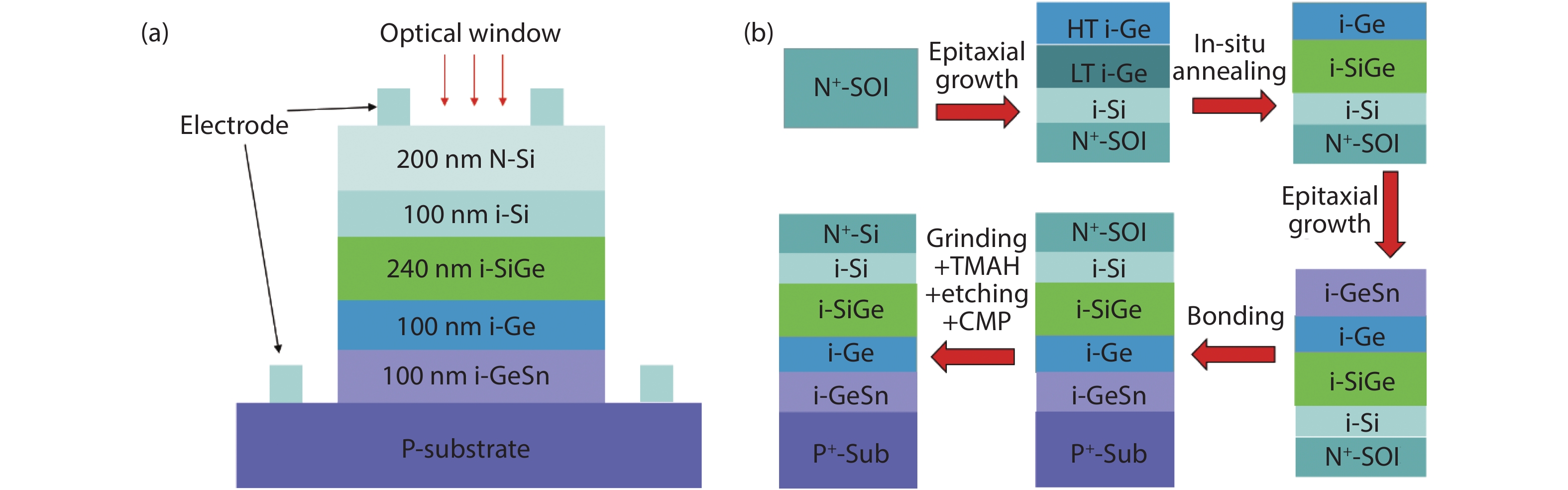
A schematic cross-section of our device structure is presented in Fig. 1(a). We superimposed the Si/graded-SiGe/ Ge/Ge0.9Sn0.1 layers on the n+-Si substrate in the order of epitaxial growth. The graded-SiGe layer was formed by in-situ annealing (the epitaxial buffer of graded-SiGe is much thicker). The device can be prepared by bonding the epitaxial layer onto a new substrate, as shown in Fig. 1(b)[
![]()
Figure 1.(Color online) (a) Schematic cross-section of the Si/graded-SiGe/Ge/Ge0.9Sn0.1 p–i–n photodetector. The mesa size is 32
2.2. Parameter setting
The Atlas simulator of the TCAD Silvaco commercial software is applied to simulate the performance of the p–i–n photodetector based on three classical equations (Poisson’s equation, continuity equation, and transport equation). According to these effective theories, we can achieve the reasonable simulation data of the designed device. Here, the temperature (T) is set to 300 K (room temperature) when some temperature dependence equations are calculated. The responsivity (R) is defined as I(g = 1)/P, and I denotes the photocurrent, g the gain, P the optical power. Optical input power of incident light source is set to 0.125 W/cm2. It is worth mentioning that there is no relevant data of GeSn in the Silvaco database. We collected the information of GeSn material, including the calculation method of bandgap[
3. Simulation results
At first, we simulated the spectral response of p–i–n photodetector with single material as the active region. Meanwhile, to compare with the result of our structure as shown in Fig. 1(a), the top layer of each photodetector was set as n+-type Si at 200 nm, both layers of p+-type and n+-type doping are set to be 1 × 1019 cm-3. The spectral response was shown in Figs. 2(a)–2(d), respectively. The material in the p+-substrate is consistent with that in the active region, as shown in Fig. 3(c). It is found that when the thickness of the active region increases gradually, the peak of responsivity shows different degrees of redshift. For example, when the thickness of the active region of Si photodetector is up to several microns, the absorption peak can be redshifted to around 800 nm. However, because we use multi-layer materials to fully combine the detection ranges, the active region of the detector becomes much thicker and this results in a greatly reduced response rate. Thus, the calculation range of each active region is set within 1000 nm.
![]()
Figure 2.(Color online) Simulation of spectral responsivity of the p–i–n photodetector with single material as active region for (a) Si, (b) graded-SiGe, (c) Ge, and (d) Ge0.9Sn0.1.
![]()
Figure 3.(Color online) (a) AES of the sample annealed at 800 °C for 30 min and 900 °C for 0 s. (b) AES of the sample annealed at 800 °C for 30 min and 900 °C for 10 min. (c) Schematic cross-section of the single material p–i–n photodetector. The mesa size is 32
To determine the variation of Ge content in graded-SiGe, the samples of Ge epitaxial growth on Si by two-step method were annealed and performed auger electron spectroscopy (AES) characterization. The phenomenon of atomic interdiffusion appears at the interface between Si and Ge[
There are two main sources of dark current density (Jdark) in the photodetector: the bulk leakage current density (Jbulk) and the surface leakage current density (Jsurf). The main source of Jsurf is the interface traps around the mesa. The interface traps can introduce energy levels in the bandgap and eventually increase the Jsurf. Both doping and TDD have a significant effect on the minority carrier lifetime (MCL) and ultimately affect the Jdark. The TDD of Si material in substrate and active region is much lower than that of epitaxial Ge. The MCL of Si is mainly affected by the doping. We set the MCL of n+-Si to 1 × 10⁻⁸ s. The MCL of Si in active region is set to 1 × 10⁻⁴ s[
![]()
Figure 4.(Color online) Simulation of
Based on this analysis, to keep the absorption peak of each material at different positions and control the thickness of the active region within a reasonable range, we superimposed Si, Ge and Ge0.9Sn0.1 from top to bottom in the active region. The thickness of each layer in the active region was set to 600 nm. We simulated the spectral response of the device as shown in Fig. 5(a). One can see that the cut-off wavelength is about 2300 nm. To flatten the response, we reduced the thickness of Ge0.9Sn0.1 from 600 to 100 nm. The responsivity at 1800 nm is reduced to about 0.57 A/W, it is still an acceptable value. To maximize the range of the flat response, we set the thickness of Ge0.9Sn0.1 to 100 nm and reduced the thickness of the Ge layer, as shown in Fig. 5(b). We find that when the thickness of Ge layer is between 100 and 200 nm, it is consistent with the tendency of flat response. Considering the contribution of the Si and graded-SiGeabsorption layers in the Vis optical signal, we set the thickness of Ge layer to 100 nm. It can be observed from Fig. 5(c) that when the thickness of the Si layer is between 0 and 600 nm, there is no significant effect on the spectral response. This happens because that the absorption coefficient of Ge is much larger than that of Si in the Vis range. A thin Si layer in active region cannot improve the responsivity of the photodetector. However, in the process of growth and annealing, i-Si plays an important role as a pure diffusion source and a barrier to resist the diffusion of doped elements from p+-substrates to the Ge layer. To match the conditions of the experiment, we set the thickness of Si layer to 100 nm. Finally, we simulated the effect of graded-SiGe layer on the spectral response when the thickness is 200 to 300 nm, as shown in Fig. 5(d). To maintain the coefficient characteristics of graded-SiGe, the thickness is controlled in some range. This suggests that when the thickness of the graded-SiGe layer is set to 240 nm, the spectral response is relatively flat. The responsivity of this photodetector is about 0.57 A/W in the range of 700 to 1800 nm.
![]()
Figure 5.(Color online) The variation of responsivity under different active region is simulated for (a) Ge0.9Sn0.1, (b) Ge, (c) Si, and (d) graded-SiGe.
In the procedure of regulating the thickness of different materials in the active region, when the thickness of the Ge0.9Sn0.1 layer is reduced from 600 to 100 nm, the Jdark is reduced from 0.22 to 0.17 mA/cm2, as shown in Fig. 6(a). When the thickness of other materials is changed, the magnitude of the Jdark remains the same. This is due to the photodetectors of pure Si, graded-SiGe, and Ge have at least two orders of magnitude lower than that in Ge0.9Sn0.1. This structure wraps a thin Ge0.9Sn0.1 layer inside the device to reduce the Jsurf and Jbulk of Ge0.9Sn0.1. This leads to a reduction in Jdark. The spectral response of the designed photodetector and the Jdark changes between 0–6 V reverse bias was shown in Fig. 6(b). This indicates that when the reverse bias is below 5 V, the Jdark remains stable.
![]()
Figure 6.(a) Magnitude of the
4. Discussion
The graded-SiGe layer is formed by annealing, the thin layer can be obtained easier and more convenient compared with the growth method. The annealing process can also minimize the dislocation in Ge material and introduce a certain tensile strain on the surface of Ge layer. This tensile strain can partially relieve compressive strain caused by large lattice mismatch in the following epitaxial of GeSn layer, thus optimizing the quality of GeSn material[
We modulate the thickness of different materials with different absorption peaks to flatten the spectral response. The absorption of Vis optical signal is enhanced by graded-SiGe and the absorption of IR optical signal is expanded by Ge0.9Sn0.1, a flat and broad response can be obtained. The thickness of graded-SiGe and Ge layer is controlled in a proper range to avoid the redshift of absorption peak. This can reduce the range and flatness of the flat response. Meanwhile, we optimized the structure to effectively mitigate the negative effects of the dead-space effect. The thickness of the active region, especially the Ge0.9Sn0.1 material, is greatly reduced, which can be helpful to reduce the dark current density.
Taking into account the actual optical signal incidence, the anti-reflection coating shows the difference in transmission on optical signals of different wavelengths[
5. Conclusions
In summary, a high-performance Si/graded-SiGe/Ge/Ge0.9Sn0.1 p–i–n photodetector with flat and broad response is achieved by theoretical study. The p–i–n photodetector consists of entirely group IV materials and reaches a responsivity as high as 0.57 A/W at a range of 700 to 1800 nm. This range covers all of the communication bands. The graded-SiGe layer formed by annealing is beneficial to improve the quality of Ge and Ge0.9Sn0.1 layer. The cut-off wavelength of the broadband photodetector is about 2300 nm, the dark-current density is as low as 0.17 mA/cm2 under a reverse bias of 3 V due to the theoretical optimization. This work shows a prospective method to fabricate broadband p–i–n photodetectors with flat response. This is of significant help to the simplification of subsequent circuits and the improvement of accuracy in the detection system, and has great importance in cost-effective integrated Si photonics.
Acknowledgements
This work was supported by National Basic Research Program of China (No. 2013CB632103), National Natural Science Foundation of China (Nos. 61534005 and 61474081), and Scientific Research Project of Fujian Provincial Department of Education (No. JA15651).
References
[1] G Eda, G Fanchini, M Chhowalla. Large-area ultrathin films of reduced graphene oxide as a transparent and flexible electronic material. Nat Nanotechnol, 3, 270(2008).
[2] S Park, G Wang, B Cho et al. Flexible molecular-scale electronic devices. Nat Nanotechnol, 7, 438(2012).
[3] F P G de Arquer, A Armin, P Meredith et al. Solution-processed semiconductors for next-generation photodetectors. Nat Rev Mater, 2, 16100(2017).
[4] X Gong, M Tong, Y Xia et al. High-detectivity polymer photodetectors with spectral response from 300 nm to 1450 nm. Science, 325, 1665(2009).
[5] H Qiao, J Yuan, Z Q Xu et al. Broadband photodetectors based on graphene–Bi2Te3 heterostructure. ACS Nano, 9, 1886(2015).
[6] H Yuan, X Liu, F Afshinmanesh et al. Polarization-sensitive broadband photodetector using a black phosphorus vertical p–n junction. Nat Nanotechnol, 10, 707(2015).
[7] W Hu, H Cong, W Huang et al. Germanium/perovskite heterostructure for high-performance and broadband photodetector from visible to infrared telecommunication band. Light: Sci Appl, 8, 106(2019).
[8] C Eckhardt, K Hummer, G Kresse. Indirect-to-direct gap transition in strained and unstrained Sn
[9] W Du, S A Ghetmiri, B R Conley et al. Competition of optical transitions between direct and indirect bandgaps in Ge1−
[10] A Gassenq, F Gencarelli, J van Campenhout et al. GeSn/Ge heterostructure short-wave infrared photodetectors on silicon. Opt Express, 20, 27297(2012).
[11] H Cong, C L Xue, J Zheng et al. Silicon based GeSn p–i–n photodetector for SWIR detection. IEEE Photonics J, 8, 1(2016).
[12] S J Su, B W Cheng, C L Xue et al. GeSn p–i–n photodetector for all telecommunication bands detection. Optics Express, 19, 6400(2011).
[13] J Mathews, R Roucka, J Xie et al. Extended performance GeSn/Si(100) p–i–n photodetectors for full spectral range telecommunication applications. Appl Phys Lett, 95, 133506(2009).
[14] J Kouvetakis, J Menendez, A V G Chizmeshya. Tin-based group IV semiconductors: New platforms for opto- and microelectronics on silicon. Annu Rev Mater Res, 36, 497(2006).
[15] S Y Ke, Y J Ye, S M Lin et al. Low-temperature oxide-free silicon and germanium wafer bonding based on a sputtered amorphous Ge. Appl Phys Lett, 112, 041601(2018).
[16] S Y Ke, Y J Ye, J Y Wu et al. Interface characteristics and electrical transport of Ge/Si heterojunction fabricated by low-temperature wafer bonding. J Phys D, 51, 265306(2018).
[17] S Y Ke, S M Lin, Y J Ye et al. Bubble evolution mechanism and stress-induced crystallization in low-temperature silicon wafer bonding based on a thin intermediate amorphous Ge layer. J Phys D, 50, 405305(2017).
[18] Y Lin, K H Lee, S Bao et al. High-efficiency normal-incidence vertical p–i–n photodetectors on a germanium-on-insulator platform: Publisher's note. Photonics Res, 6, 46(2018).
[19] S A Ghetmiri, W Du, B R Conley et al. Shortwave-infrared photoluminescence from Ge1–
[20] H Tran, W Du, S A Ghetmiri et al. Systematic study of Ge1−
[21] C Masini, L Calace, G Assanto et al. High-performance p–i–n Ge on Si photodetectors for the near infrared: From model to demonstration. IEEE Trans Electron Devices, 48, 1092(2001).
[22] M Rzaev, F Schäffler, V Vdovin et al. Misfit dislocation nucleation and multiplication in fully strained SiGe/Si heterostructures under thermal annealing. Mater Sci Semicond Process, 8, 137(2005).
[23] J Humlíček, M Garriga, M I Alonso et al. Optical spectra of Si
[24] R Braunstein, A R Moore, F Herman. Intrinsic optical absorption in germanium-silicon alloys. Phys Rev, 109, 695(1958).
[25] D Choi, Y S Ge, J S Harris et al. Low surface roughness and threading dislocation density Ge growth on Si (001). J Cryst Growth, 310, 4273(2008).
[26] G Xia, J L Hoyt, M Canonico. Si –Ge interdiffusion in strained Si/strained SiGe heterostructures and implications for enhanced mobility metal–oxide–semiconductor field-effect transistors. J Appl Phys, 101, 044901(2007).
[27] M Gavelle, E M Bazizi, E Scheid et al. Study of silicon-germanium interdiffusion from pure germanium deposited layers. Mater Sci Eng B, 154/155, 110(2008).
[28] H Luan, D R Lim, K K Lee et al. High-quality Ge epilayers on Si with low threading-dislocation densities. Appl Phys Lett, 75, 2909(1999).
[29] J del Alamo, S Swirhun, R M Swanson. Simultaneous measurement of hole lifetime, hole mobility and bandgap narrowing in heavily doped n-type silicon. Int Electron Devices Meet, 290(1985).
[30] S S Kulin, A D Kurtz. Effect of dislocations on minority carrier lifetime in germanium. Acta Metall, 2, 354(1954).
[31] Y Zhao, N Wang, K Yu et al. High performance silicon-based GeSn p–i–n photodetectors for short-wave infrared application. Chin Phys B, 28, 128501(2019).
[32]
[33] C Chang, Y D Sharma, Y Kim et al. A surface plasmon enhanced infrared photodetector based on InAs quantum dots. Nano Lett, 10, 1704(2010).
[34] J K Yang, M K Seo, I K Hwang et al. Polarization-selective resonant photonic crystal photodetector. Appl Phys Lett, 93, 211103(2008).
[35] T F Zhu, Z C Liu, Z C Liu et al. Fabrication of monolithic diamond photodetector with microlenses. Opt Express, 25, 31586(2017).
[36] H Zhong, A R Guo, G H Guo et al. The enhanced light absorptance and device application of nanostructured black silicon fabricated by metal-assisted chemical etching. Nanoscale Res Lett, 11, 1(2016).


Set citation alerts for the article
Please enter your email address

© Copyright 2018-2021 | Chinese Laser Press. All Rights Reserved 沪ICP备15018463号-20