
Weijun Wang, Liang-Hui Du, Jiang Li, Pei-Ren Tang, Changlin Sun, Songlin Chen, Jun Wang, Zhao-Hui Zhai, Zhipeng Gao, Ze-Ren Li, Jianquan Yao, Furi Ling, Li-Guo Zhu. Terahertz wave avalanche breakdown transistor for high-performance switching[J]. Photonics Research, 2021, 9(3): 370
- Photonics Research
- Vol. 9, Issue 3, 370 (2021)
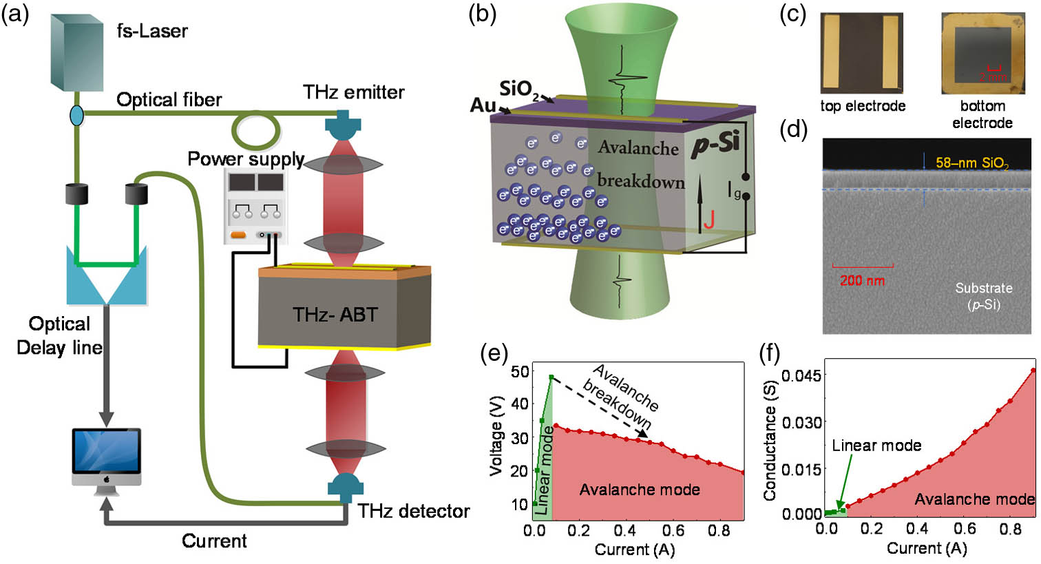
Fig. 1. Circuitry diagram of the setup, device properties, concept, and performance of our avalanche transistor THz modulator. (a) The THz-TDS system schematic and the experimental setup. (b) Schematic illustration of the device. (c) Top electrode, bottom electrode of the avalanche transistor. (d) Scanning electron micrograph (SEM) of the device section. (e) The I –V characteristic curve of the avalanche transistor in the linear and avalanche modes. (f) The corresponding I –G curve.
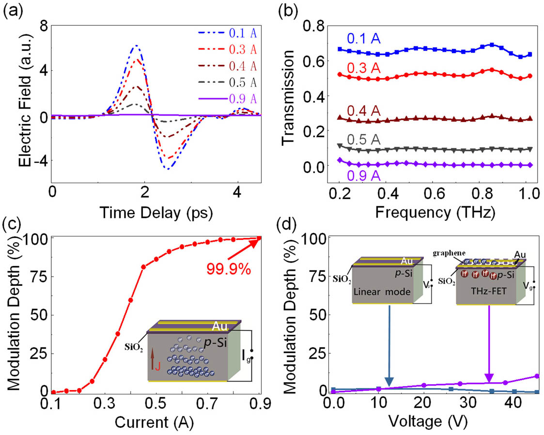
Fig. 2. Performance of the avalanche transistor THz switcher and its comparison with devices in the linear mode or using THz-FET effect. (a) Time-domain THz signals under different currents in the avalanche mode. (b) The calculated frequency-domain transmission of THz waves at currents of 0.1 A, 0.3 A, 0.4 A, 0.5 A, and 0.9 A in the avalanche mode. (c) The corresponding MD of the avalanche transistor under different currents in the avalanche mode at 0.7 THz. (d) The transmissions of our device in the linear mode and a conventional monolayer graphene field-effect transistor (FET) with the same thickness of p
Fig. 3. Calculated electrical properties of p p
Fig. 4. Modulation speed of the avalanche transistor device. (a) The experimental setup. The normalized MD of CW THz wave driven by a square-wave modulated illumination laser (b) at the rate of 1 kHz and (c) at the rate of 12 kHz. (d) Normalized MD magnitude at different modulation frequencies, showing a 3 dB operation bandwidth about 12 kHz.
Fig. 5. Device preparation lithography flow chart.
Fig. 6. (a) Schematic to obtain the I –V characteristic of bare p I –V curve of p
Fig. 7. Photo of experimental setup for the avalanche transistor THz modulator.
Fig. 8. Time-domain THz signals under different currents in the avalanche mode.
Fig. 9. (a) Forth-back I –G curve of the avalanche breakdown transistor (ABT) in the avalanche breakdown mode. (b) The forth-back modulation depth of the THz-ABT device.
Fig. 10. Behaviors of the THz-ABT device in the reflection configuration. (a) The measurement schematic for reflection configuration. (b) The time-domain signals under different biased currents. (c) The zoomed-in THz waveforms of the peak area of E r 1 in (b). (d), (e) The measured and simulated reflection coefficients in the frequency domain under different biased currents.
Fig. 11. Conductivities of the THz-ABT device under different currents by setting different carrier collision frequency.
Fig. 12. (a) Measured (circle) and theoretical (solid curve) values of the transmission spectra of the THz-ABT at 0.1 A, 0.3 A, 0.4 A, 0.5 A, and 0.9 A in the avalanche mode. (b) The corresponding modulation depth of theoretical values. The behavior of the THz-ABT is well explained by the built theoretical model.
Fig. 13. (a), (b) Real and imaginary parts of permittivity of p
Fig. 14. Schematic of the experimental configuration for dynamic modulation measurements.
Fig. 15. (a) Normalized modulation magnitude at different modulation frequencies, showing a − 3 dB − 3 dB
|
Table 1. Comparison of the THz Devices Performance of Amplitude Modulation Depth

Set citation alerts for the article
Please enter your email address
© Copyright 2018-2021 | Chinese Laser Press. All Rights Reserved 沪ICP备15018463号-20