There is still a lack of high-performance terahertz (THz) modulators with wide operation bandwidth and large modulation depth due to the underlying physics limitation behind existing approaches. Meanwhile, for many applications, simple compact THz modulators working straightforward in the transmission mode are also highly desired. Here, we demonstrate a THz modulator with a maximal transmission-amplitude modulation depth of 99.9% (switching ratio of 1000) based on a commonly used silica-on-silicon structure. Different from those reported graphene or metamaterials enhanced proposals, the device we proposed works within a reversible avalanche breakdown region of silicon that has not been studied yet and has the potential to modulate/switch THz waves efficiently. Further, we proved that the modulation depth exceeds 97% in the frequency range from 0.2 to 1 THz in the experiment. The simplicity and generality of this new type of near-perfect THz modulator will undoubtedly attract lots of attention of researchers in the near future due to its potential to be engineered into integrated devices.
1. INTRODUCTION
Active modulators providing the means to manipulate terahertz (THz) waves are one of the important and desirable components in the applications of THz science [1–4]. Tremendous efforts have been devoted to developing efficient THz modulators based on 2DEG, metamaterials, and phase transition materials or photon-injection schemes [5–15]. However, the reported THz modulators are restricted by limitations in terms of modulation depth (MD)/switching ratio (SR), narrowband response, insertion loss (IL), or processing/configuration complexity [16–23]. The SR refers to the ratio of the maximum transmission amplitude to the minimum transmission amplitude through the device. For example, the metamaterial-enhanced THz modulators can only work in a bandwidth about 0.25 THz due to the intrinsic limited bandwidth resonance property of metamaterial [17]. The semiconductor hybrid structures are usually utilized to broaden the operation bandwidth, such as graphene on silicon (GOS) and on silicon, but these structures need extra material deposition processes. The GOS semiconductor hybrid structure is commonly used as the electrical tunable THz modulator, while the amplitude MD/SR can only reach about 91.6%/12 in the attenuated total reflectance (ATR) configuration due to the limited tunable range of the graphene’s Fermi level [8]. Setting the incident angle as the Brewster angle can further improve the SR to about 32, but this strategy suffers from the high IL due to the inevitable high Fresnel reflection loss [5]. At the same time, the ATR or Brewster angle configuration also complicates the system’s setup. The optical tunable GOS structures overcome this high IL disadvantage, but these architectures require the assistance of additional high-power optical pumping acting as the major obstacle for their practical applications [12–16]. Thus, high-performance THz modulators working in the simple electrical tunable transmission mode with high MD, broad operation bandwidth, and small IL are still in great demand.
The silicon–silica structure is the most widely used one in the semiconductor industry. However, previous reports claimed that the typical MD of this structure is almost 0 using electrical tuning methods [10,21]. While pumped by continuous wave (CW) laser with a power of , this structure () can only reach around 20% in the THz range [16], making it unsuitable to demonstrate high-performance modulators. Thus, this silicon–silica structure is usually used as the substrate of functional modulator materials other than the modulator itself [5,6]. In this work, a high-performance THz modulator scheme was proposed based on the untapped avalanche breakdown transistor (ABT) effect of the conventional structure. By gradually increasing the gate voltage of the device to a critical value, the device transits from the usual linear mode to a remarkable reversible avalanche breakdown mode. In the avalanche breakdown mode, the conductance of the devices changes steeply, and increasing the gate current leads to a dramatic attenuation of the incident THz wave in the meanwhile. The maximal transmission-amplitude MD is about 99.9% by gradually increasing from 0.1 to 0.9 A. The MD is slightly dependent on the operation frequency and remains larger than 97% in the concerned frequency range from 0.2 to 1.0 THz. The IL of our proposed THz modulator is around 3 dB, which mostly attributes to the Fresnel reflection loss at the interfaces of our devices. Here, the IL is defined as , with being the initial transmission amplitude when no voltage is applied. The mechanism of our THz modulator is investigated in detail. The carrier multiplications process in silicon accompanying the avalanche transistor effect of the devices is the main cause of the severe absorption of THz waves. The Drude model is used to theoretically explain the modulation performances of our THz modulator, and it agrees pretty well with experimental data. Finally, we present a comparison between the performances of the proposed THz-ABT modulator. We found the overall performance of the THz-ABT modulator is excellent considering the simple configuration and fabrication of this device.
2. STRUCTURE AND CONCEPTS
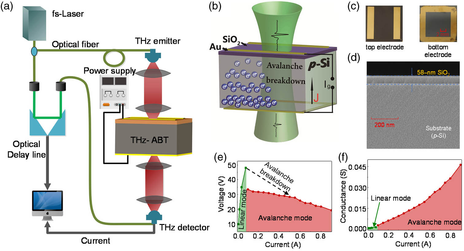
Figure 1 shows our experimental setup [Fig. 1(a)] and a schematic of our proposed avalanche transistor THz modulator [Fig. 1(b)]. The device simply consists of a 300 μm low-resistivity () -Si substrate with a 58 nm silicon oxide insulator layer on top. As shown in Fig. 1(c), two square metal strips were carefully placed onto one side of silicon as top electrodes, and silicon removed the native oxide layer by soaking it in hydrofluoric acid before plating the bottom electrode (see Appendix A, Fig. 5). Then 58 nm thick silicon dioxide was deposited on the other side of silicon. The average thickness of is approximately 58 nm, characterized by cross-sectional scanning electron microscopy as illustrated in Fig. 1(d). The square electrode has a side length of 12 mm and a width of 2 mm, and the area of the uncovered electrode in the middle is . TiAu electrodes were deposited on both sides of the device to apply the manipulation voltage. As the gate voltage gradually increases to about 50 V, the current is linearly increasing with small amplitude noted as the linear mode. After that sudden increase of the current and decrease of gate voltage were observed, as indicated by a black dashed arrow in Fig. 1(e). The corresponding conductance is steeply increased, as illustrated in Fig. 1(f). This extraordinary phenomenon means the silicon was entering the reversible avalanche mode [24–28]. The avalanche breakdown of silicon refers to the phenomenon that the current as well as the total power increases exponentially at a critical voltage (see Appendix B, Fig. 6)
Sign up for Photonics Research TOC. Get the latest issue of Photonics Research delivered right to you!Sign up now
Figure 1.Circuitry diagram of the setup, device properties, concept, and performance of our avalanche transistor THz modulator. (a) The THz-TDS system schematic and the experimental setup. (b) Schematic illustration of the device. (c) Top electrode, bottom electrode of the avalanche transistor. (d) Scanning electron micrograph (SEM) of the device section. (e) The I–V characteristic curve of the avalanche transistor in the linear and avalanche modes. (f) The corresponding I–G curve.
Figure 2.Performance of the avalanche transistor THz switcher and its comparison with devices in the linear mode or using THz-FET effect. (a) Time-domain THz signals under different currents in the avalanche mode. (b) The calculated frequency-domain transmission of THz waves at currents of 0.1 A, 0.3 A, 0.4 A, 0.5 A, and 0.9 A in the avalanche mode. (c) The corresponding MD of the avalanche transistor under different currents in the avalanche mode at 0.7 THz. (d) The transmissions of our device in the linear mode and a conventional monolayer graphene field-effect transistor (FET) with the same thickness of -type silicon and silicon dioxide as the avalanche transistor under different voltages.
Figure 3.Calculated electrical properties of -silicon in the avalanche mode. (a), (b) The real and imaginary parts of permittivity of -silicon under different gate currents in the frequency domain. (c), (d) The derived conductivity/carrier concentration as well as the plasma frequency.
Figure 4.Modulation speed of the avalanche transistor device. (a) The experimental setup. The normalized MD of CW THz wave driven by a square-wave modulated illumination laser (b) at the rate of 1 kHz and (c) at the rate of 12 kHz. (d) Normalized MD magnitude at different modulation frequencies, showing a 3 dB operation bandwidth about 12 kHz.
In the linear mode, the power supply acts as the constant voltage source and the current of the device also slightly increases with the applied gate voltage. In this mode, the total resistance of the device is quite large mainly contributed by the silicon oxide insulator. As the voltage approaches a critical value of about 50 V, a tunneling effect occurs in the silicon dioxide layer leading to an abrupt decrease of its resistance, and the voltage dropped on the silicon increases dramatically at this situation. As a consequence, -silicon enters the avalanche breakdown zone. Considering the power supply we used has a protecting value of the total output power, the device transits to the avalanche mode with the gate voltage drastically reduced and the current reaching a balanced value. In this avalanche mode, the power supply acts as a constant current mode. Thus, the current of the device was tuned to electrically manipulate its performance. Next, the current was carefully tuned from the avalanche breakdown point back to about 0.1 A and it is still working at the avalanche mode. Then, the current was gradually tuned up from 0.1 to 0.9 A. The corresponding gate voltage decreases as the current increases.
3. PERFORMANCE CHARACTERISTIC
A home-made THz time-domain spectroscopy (TDS) system was used to measure the transmission spectra of the device under different current in the avalanche mode [Fig. 1(a)]. The incident angle of the linearly polarized THz pulse is set to be 0°. The THz waves were generated via an InGaAs photoconductive antenna (PCA) under bias voltage, which was pumped by fiber laser pulses (central wavelength of 1560 nm, repetition rate of 100 MHz, and pump power of ). The size of the focused spot was approximately 2 mm through a system (two lenses with identical focal lengths of 50 mm). In the meantime, THz waves were coherently detected by another PCA with detection power of . The signal of the terahertz receiving antenna was recorded by the lock-in amplifier and transmitted to the computer [7]. The signal-to-noise ratio (SNR) of our THz-TDS system is larger than 1000:1 and the bandwidth of THz-TDS is from 0.2 to 1.0 THz [20]. Our device was located where the terahertz wave was focused to measure the modulation effect (see Appendix C, Fig. 7). This high SNR is significant to obtain the accurate THz signal with small amplitude especially in the situation of large current. Figure 2(a) shows the measured time-domain THz signal of the device under different currents in the avalanche mode. It was observed that the increased current caused significant attenuation of the transmitted THz pulse. As shown in Fig. 2(a), under the current of 0.9 A, the amplitude of the transmitted THz pulse almost disappeared, which indicates the modulation depth of our THz modulator is pretty high. Meanwhile, we also investigated corresponding transmission spectra of our device at the currents of 0.1, 0.3, 0.4, 0.5, and 0.9 A, respectively, as shown by the open markers in Fig. 2(b). At the current of 0.9 A, the transmission spectrum is nearly zero in a wide frequency range. The transmission of our devices is obtained using the formula , where and are Fourier transformed from the time-domain signal transmitted through the sample and air, respectively. In order to avoid Fabry–Perot oscillations, we keep the first transmitted THz pulse with the help of a window function (see Appendix C, Fig. 8).
Figure 2(c) represents the MD of the avalanche transistor under the current from 0.1 to 0.9 A in the avalanche mode at 0.7 THz. It can be seen that as the current gradually increases, the transmission of the avalanche transistor is decreased. The MD approaches 1 when the current is 0.9 A. Here, the MD and SR are defined as and , respectively, where and are the transmission under gate current of 0.1 A and at 0.7 THz, respectively. The maximum MD of our avalanche transistor 99.9% (SR of 1000) was achieved when 0.9 A current applied in our experiment. In the meantime, by moving the device so that the THz wave passes through different positions of the device, we find that the MD of the THz wave has not changed. For a comparison, Fig. 2(d) shows the transmission of avalanche transistor under different voltages in the linear mode; it was found that the MD is around 0 for the linear mode. The MD is near 0 in the linear mode, which is due to the fact that conductivity of the transistor is fairly low and the conductivity change is negligible in this mode. We also fabricated a commonly used monolayer graphene field-effect transistor (FET) with the same thickness of -type silicon and silicon dioxide as the avalanche transistor. We found that the transmission change of the THz-FET modulator in the linear mode is less than 10% considering the limited carrier concentration adjustment of monolayer graphene by applying a biased gate voltage [29]. Therefore, the avalanche transistor shows a strong application prospect as a high-performance THz modulator.
The change trend of MD is consistent with the measured I–V characteristic of the device. As the gate current increases in the avalanche mode, the conductivity and the MD of the devices increase (see Appendix C, Fig. 9), meaning the carrier concentration density in the -silicon also increases. Thus, the transmission of THz waves is attenuated due to the absorption and the reflection and the MD becomes larger. After it reaches 0.9 A, the gate voltage turns down and the transmission of THz increases with smaller and smaller MD. When the current approaches 0.9 A, a saturation phenomenon of MD is observed [18]. The back and forth tuning of the gate current shows that the performance of the avalanche transistor is reversible. In the meantime, we also found that when changing the direction of the gate voltage, the modulation effect is basically the same. This result implies that the carrier density of the avalanche transistor is only related to the value of the current and is independent of the direction of the gate current.
Figure 9.(a) Forth-back I–G curve of the avalanche breakdown transistor (ABT) in the avalanche breakdown mode. (b) The forth-back modulation depth of the THz-ABT device.
From the THz-TDS signals, we know that the modulation is not an interface but a bulk effect (see Appendix D, Fig. 10). Thus, the -silicon of our avalanche transistor should be treated as a bulk, and the transmission of the THz pulse can be simply expressed as where and are the complex refractive index and the complex permittivity of -silicon, respectively. is the angular frequency of the THz wave, is the vacuum light speed, and μ is the thickness of -silicon. Here, the Drude model was used to describe the complex permittivity of -silicon, where is the constant permittivity at the infinite frequency, is the conductivity of -silicon at direct current (DC), is the carrier collision frequency, and is the vacuum permittivity [30,31]. With the above formula, we can fit the transmission spectrum and obtain the parameter under different gate currents (details of the fitting of the transmission spectra can be found in Appendix E, Table 2, Figs. 11 and 12) [32,33]. The experimental and theoretical data agree well with each other, indicating that the behavior of the avalanche transistor can be well explained by the bulk effect of -silicon. As shown in Fig. 3(a), the real part of permittivity decreases as the gate current becomes larger, which explains the THz signal gradually increasing at the reflection configuration [see Appendix D, Figs. 10(b) and 8(c)]. In the meantime, the imaginary part of permittivity of -silicon becomes larger and larger, indicating that the absorption is increased as well as deeper and deeper MD of the THz wave. As the imaginary part of the permittivity increases, there is an increasing impedance mismatch with the surrounding air resulting in increased reflection [24]. In the high-THz frequency region, the modulation of the device will gradually decrease as the frequency increases. The device has a high modulation depth of over 90% at 0.2–2.3 THz, which shows excellent potential (see Appendix E, Fig. 13).
Figure 10.Behaviors of the THz-ABT device in the reflection configuration. (a) The measurement schematic for reflection configuration. (b) The time-domain signals under different biased currents. (c) The zoomed-in THz waveforms of the peak area of Er1 in (b). (d), (e) The measured and simulated reflection coefficients in the frequency domain under different biased currents.
Figure 12.(a) Measured (circle) and theoretical (solid curve) values of the transmission spectra of the THz-ABT at 0.1 A, 0.3 A, 0.4 A, 0.5 A, and 0.9 A in the avalanche mode. (b) The corresponding modulation depth of theoretical values. The behavior of the THz-ABT is well explained by the built theoretical model.
Figure 13.(a), (b) Real and imaginary parts of permittivity of -silicon under different gate currents in the frequency range 0.2–4 THz. (c) Theoretical transmission spectra of the THz-ABT at 0.1 A, 0.3 A, 0.4 A, 0.5 A, and 0.9 A in the avalanche mode at 0.2–4 THz. (d) The corresponding modulation depth of theoretical values.
In order to further understand the avalanche breaking down process of -silicon, we also investigate the relationships between the DC conductivity, the carrier density of -silicon, and the gate current, shown in Fig. 3(c). The relationship between the conductivity and the carrier density is determined by , where is the effective mass of the carrier in -silicon [30,34]. It can be seen that the conductivity and the carrier density increase with the gate current. These results are consistent with the measured conductivity of the device in the avalanche mode. At the currents of 0.1 and 0.9 A, the carrier’s densities are about and , which is still in a reasonable range for -silicon.
The plasma frequency has also been calculated, as illustrated in Fig. 3(d) [31]. We found that the plasma frequency is of the same order of the concerned THz range. Thus, strong absorption of the incident THz wave is expected [35], which is essential for a broadband THz modulator. Conversely, when the current decreases, the carriers decrease and result in a lower MD. So the dynamic modulation can be done by changing the gate current.
5. MODULATION WITH PHOTON INJECTION
As analyzed above, in the avalanche mode, the modulation mechanism of the avalanche transistor is using the gate current to adjust the carrier concentration injected into the -silicon. As more carriers are injected, the total current becomes larger and results in a higher MD of the THz wave. Conversely, when the current decreases, the injected carriers decrease and result in a lower MD. So the dynamic modulation can be done by changing the gate current or the injection of carriers.
In this section, we use the photon-doping method as a straightforward way to inject the carriers [see Appendix F, Figs. 14 and 15]. As illustrated in Fig. 4(a), the dynamic modulation characteristic performance of the THz-ABT modulator was measured at 220 GHz carrier. A square-wave voltage was applied to the acousto-optic modulator to tune the power of the photon-doping laser between 0 and 100 mW. The state of the device is in the avalanche mode with a gate current of 0.3 A. A typical normalized MD of THz transmission at the modulation frequency of 1 kHz is given in Fig. 4(b). Figure 4(c) gives the normalized MD of the THz-ABT when the modulation frequency turns up to 12 kHz. The normalized MD is decreased to about 3 dB at this modulation frequency. The normalized MD magnitude of the THz-ABT at different modulation frequencies was summarized in Fig. 4(d), which indicates a 3 dB operation bandwidth is .
Figure 14.Schematic of the experimental configuration for dynamic modulation measurements.
Figure 15.(a) Normalized modulation magnitude at different modulation frequencies, showing a operation bandwidth at the current of 0.2 A. (b) The operation bandwidth at the current of 0.4 A.
As shown in Table 1, we compare our THz-ABT modulator with other reported THz modulators based on different materials and different modulation types including the THz-FET, diode, and photon-doping devices. All the devices are based on a similar mechanism by tuning the carrier density to modulate THz waves. The SR of our proposed THz-ABT modulator is more than 5 times larger than the reported works. Meanwhile, our THz-ABT modulators can work in the simple electrical tunable transmission mode with the commonly used silica-on-silicon structure.
Comparison of the THz Devices Performance of Amplitude Modulation Depth
Material
Modulation Type
Measured Frequency [THz]
THz Modulation Depth [%]
THz Switch Ratio
Modulation Speed
Reference
Si
THz-ABT
0.2–1
99.9
1000
12 kHz
This work
Graphene-Si, ATR
THz-FET
0.15–0.4
91.64
11.96
—
[8]
Silicon nanotip array
Photon injection
0.25–1
78.15
4.58
—
[12]
Graphene-
Brewster angle, THz-FET
0.5–1.6
96.9
32.26
[5]
Photon injection
0.3–0.5
99.5
200
—
[14]
Graphene/Si
Photon injection
0.2–2.0
99
100
—
[15]
Phthalocyanine compound/Si
Photon injection
0.2–2.6
99
100
—
[36]
Photon injection
0.2–2.6
99
100
—
[16]
Si-Plasmonic gold nanoparticles
Photon injection
0.1–1.0
70
3.33
—
[13]
Graphene-Si
Diode, photon injection
0.4–2.0
83
5.88
—
[10]
Graphene/Si
THz-FET
0.57–0.63
15
1.17
20 kHz
[21]
Composite metamaterial
Heterostructure
0.351
85
6.67
0.2 GHz
[37]
Based on the THz-ABT effect, we achieved to switch the THz wave with SR about 1000, which is more than 5 times larger than previous results. The IL has an acceptable value of about 3 dB. In this paper, a new type of THz modulator based on the avalanche breakdown effect of semiconductor has been proven with the ability of achieving the near-perfect MD. It is also worth mentioning that this THz-ABT device can work in the simple transmission mode, which can be applied in vast fields of THz science. The simplicity and convenience of this THz-ABT modulator will undoubtedly attract more and more attention of researchers in the near future.
APPENDIX A: FABRICATION PROCESS OF THE DEVICE
As illustrated in Fig.?5, the silicon wafer was cleaned and then a silicon dioxide layer with a surface of 58?nm was obtained by a thermal dry oxygen oxidation method. Then, the natural silicon dioxide layer at the bottom of the silicon wafer was removed by the silicon wafer polishing method. This was followed by photolithography, sputtering, and deposition of a metal film to obtain the bottom electrode, and then the same method was used to obtain the top electrodes.
APPENDIX B: I–V CURVE OF P-Si
As shown in Fig.?6(a), two metallic electrodes were carefully deposited onto both sides of the -Si to obtain its I–V performance. The native oxide layer -Si is removed by soaking it into the hydrofluoric acid before depositing the electrodes. By increasing the voltage, the linear area and avalanche region with different resistive behaviors of -Si are recorded. In the avalanche region, a slight increase of the voltage leads to a steep increase of current indicating that the conductance of -Si changes greatly in this region, as shown in Fig.?6(b). The nonlinear behavior of -Si in the avalanche region, known as the avalanche breakdown phenomena, depends upon the concentration of the majority and minority impurities. Under the influence of the strong electric field, some valence electrons of the majority impurities gain sufficient energy to produce new electron–hole pairs. These newly generated carriers collide with other valence electrons after acceleration by the applied electric field, which results in more and more electron–hole pairs. This chain reaction results in a great increase of the carrier density known as the avalanche breakdown phenomenon [24].
APPENDIX C: EXPERIMENTAL SETUP AND SIGNALS PROCESSING
The experimental instruments from left to right in Fig.?7 are the power supply, TDS system test part, computer, and TDS system host. The power supply we used is a purchased product; the model is Aim-tti EX752M. We built the THz-TDS system.
As shown in Fig.?8, in order to avoid Fabry–Perot oscillations, we keep the first transmitted THz pulse with the help of a window function.
The forth-back characteristic of the I–G curve as well as the MD of the proposed THz-ABT device are given in Fig.?9. The current increased from 0.1 to 0.9?A and then decreased to its original value, and this process repeated about 50 times. We found that the behavior of -Si in the avalanche mode is reversible, and the MD performance is almost the same for every repeated process.
APPENDIX D: BULK EFFECT OF THE P-Si
Here, we use a reflection configuration to confirm that the modulation depth of our device is mainly due to the bulk effect of the -Si. The linearly polarized THz wave was incident from the air to the device at an incident angle of 40°. As the current increases, the amplitude of the first reflected THz echo increases slightly, while that of the second echo shows a significant attenuation, as illustrated in Fig.?10(b). Since the first echo is mainly affected by the air/Si interface, while the second echo has both interface and bulk contributions, the different behaviors of the first and second reflect THz echo confirm that the modulation depth effect of THz-ABT devices is mainly due to the bulk effect. As shown in Fig.?10(d), the signal-to-noise ratios of the reflection curves are not high, because of only intercepting the first peak in the time-domain signals to avoid the effect of the second peak.
APPENDIX E: FITTING OF THE TRANSMISSION SPECTRA
The conductivities of the THz-ABT device under different currents were obtained using the least-squares fitting method [Eqs.?(1)–(3)]. Because the fitted carrier collision frequency is larger than our highest measurement frequency, the carrier collision frequency is set to a fixed value. The results show that the fixed carrier collision frequency does not affect the fitting effect of conductivity, indicating that this method is feasible. is the carrier collision frequency in Table?2, and all fitted values have confidence levels above 95%. The error bars of the data points are the confidence interval obtained by fitting the transmission spectra to the Drude model.
Fitted Conductivity under Different Currents
Current (A)
0.1
0.15
0.2
0.25
0.3
0.35
0.4
0.45
Conductivity (S/m)
[3.860, 4.946]
[4.653, 5.759]
[4.674, 5.744]
[8.920, 10.016]
[19.908, 21.060]
[35.581, 37.010]
[63.489, 65.847]
[108.622, 114.893]
Current (A)
0.5
0.55
0.6
0.65
0.7
0.75
0.8
0.9
Conductivity (S/m)
[130.414, 135.922]
[158.037, 165.542]
[183.398, 193.130]
[204.035, 216.983]
[222.832, 239.110]
[260.221, 287.165]
[266.209, 295.433]
[297.781, 338.097]
As shown in Fig.?11, we choose three different values of collision frequencies to evaluate its influence on conductivity of THz-ABT devices and no obvious changes are observed, indicating that the carrier collision frequency plays a slight role in THz-ABT devices [32].
In order to get the transmission spectra at high frequency, we use Eqs.?(1), (2), and (3) for fitting. As shown in Figs.?13(a) and 13(b), the real part and the imaginary part of permittivity change become smaller with the increasing frequency of 0.2–4?THz. As the frequency increases, the real part of permittivity gradually increases, leading to the THz signal gradually decreasing at the reflection configuration. In the meantime, the imaginary part of permittivity decreases with the increase of frequency, indicating that the absorption is decreased and the MD of the THz wave becomes lower. Therefore, the change of the permittivity under increasing frequency gradually decreases, indicating that the modulation effect is weakening. In Figs.?13(c) and 13(d), as the frequency increases, the modulation effect will gradually decrease in the frequency range of 0.2–4?THz. The modulation depth maintains a high modulation depth of over 90% at 0.2–2.3?THz. This shows that the modulator also has broad application space in the terahertz high-frequency region.
APPENDIX F: EXPERIMENTAL DETAIL FOR PHOTON INJECTION
The optical setup for operation modulation is shown in Fig.?14, in which the dynamic modulation of the THz-ABT modulator was measured by 220?GHz carriers. A square-wave voltage was applied to the acousto-optic modulator to tune the power of photon-doping laser.
As can be seen from Fig.?15, there is no significant change in the modulation speed for different biased currents of the THz-ABT device.