• Photonics Research
  • Vol. 6, Issue 5, 409 (2018)
Yue Li1、2、3, Jian Li1、2、3, Taixing Huang1、2、3, Fei Huang1、2、3, Jun Qin1、2、3, Lei Bi1、2、3, Jianliang Xie1、2、3, Longjiang Deng1、2、3、4, and Bo Peng1、2、3、*
Author Affiliations
  • 1National Engineering Research Center of Electromagnetic Radiation Control Materials, University of Electronic Science and Technology of China, Chengdu 610054, China
  • 2State Key Laboratory of Electronic Thin Films and Integrated Devices, University of Electronic Science and Technology of China, Chengdu 610054, China
  • 3Key Laboratory of Multi-Spectral Absorbing Materials and Structures of Ministry of Education, University of Electronic Science and Technology of China, Chengdu 610054, China
  • 4e-mail: denglj@uestc.edu.cn
  • show less
    DOI: 10.1364/PRJ.6.000409 Cite this Article Set citation alerts
    Yue Li, Jian Li, Taixing Huang, Fei Huang, Jun Qin, Lei Bi, Jianliang Xie, Longjiang Deng, Bo Peng. Active macroscale visible plasmonic nanorod self-assembled monolayer[J]. Photonics Research, 2018, 6(5): 409 Copy Citation Text show less
    (a) SEM image of Au NRs on quartz substrate. (b) Experimental absorption spectra of Au NRs dispersed in solution (black, left axis) and deposited on quartz substrate (blue, right axis). The inset is the photograph of Au NRs deposited on quartz substrate (left) and one blank quartz substrate (right). (c) Schematic of Au NRs on quartz substrate coated by VO2 films. (d) The comparison of experimental absorption spectra for Au NRs (black), Au/VO2 hybrid films (blue), and bare VO2 films (red) on quartz substrate, respectively. (e) X-ray diffraction pattern and (f) AFM 3D image of VO2 films deposited on quartz substrate.
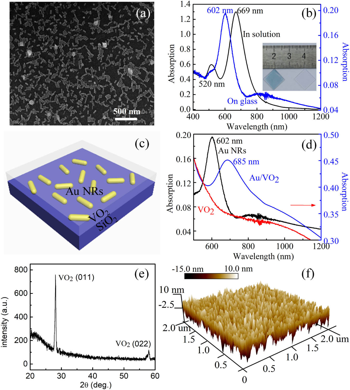
    Fig. 1. (a) SEM image of Au NRs on quartz substrate. (b) Experimental absorption spectra of Au NRs dispersed in solution (black, left axis) and deposited on quartz substrate (blue, right axis). The inset is the photograph of Au NRs deposited on quartz substrate (left) and one blank quartz substrate (right). (c) Schematic of Au NRs on quartz substrate coated by VO2 films. (d) The comparison of experimental absorption spectra for Au NRs (black), Au/VO2 hybrid films (blue), and bare VO2 films (red) on quartz substrate, respectively. (e) X-ray diffraction pattern and (f) AFM 3D image of VO2 films deposited on quartz substrate.
    Experimental absorption spectra of bare VO2 and Au/VO2 films as a function of temperature. Heating [(a), (c)] and cooling [(b), (d)] on bare VO2 [(a), (b)] and Au/VO2 [(c), (d)] films. The arrows in (c) and (d) indicate the moving direction of the plasmonic peak with the change of temperature (red: heating; blue: cooling).
    Fig. 2. Experimental absorption spectra of bare VO2 and Au/VO2 films as a function of temperature. Heating [(a), (c)] and cooling [(b), (d)] on bare VO2 [(a), (b)] and Au/VO2 [(c), (d)] films. The arrows in (c) and (d) indicate the moving direction of the plasmonic peak with the change of temperature (red: heating; blue: cooling).
    (a), (b) Longitudinal plasmon resonance peak of Au/VO2 films as a function of temperature. (c) Temperature hysteresis curves for the plasmon resonance peak of Au/VO2 films. (d) Temperature hysteresis curves for the absorption variation (relative to the absorption intensity of 0.35) of bare VO2 and Au/VO2 films, taken at 685 nm.
    Fig. 3. (a), (b) Longitudinal plasmon resonance peak of Au/VO2 films as a function of temperature. (c) Temperature hysteresis curves for the plasmon resonance peak of Au/VO2 films. (d) Temperature hysteresis curves for the absorption variation (relative to the absorption intensity of 0.35) of bare VO2 and Au/VO2 films, taken at 685 nm.
    Raman spectra of bare VO2 [(a), (c)] and Au/VO2 [(b), (d)] films at different temperatures under optical pumping by 532 nm laser with the power of 0.2 mW [(a), (b)] and 0.5 mW [(c), (d)]. The black arrows represent the change of the temperature.
    Fig. 4. Raman spectra of bare VO2 [(a), (c)] and Au/VO2 [(b), (d)] films at different temperatures under optical pumping by 532 nm laser with the power of 0.2 mW [(a), (b)] and 0.5 mW [(c), (d)]. The black arrows represent the change of the temperature.
    Raman spectra of bare VO2 and Au/VO2 films at different power by 532 nm laser. (a)–(e) Comparison of Raman spectra between bare VO2 (black) and Au/VO2 (red) films at 0.2, 0.4, 0.5, 0.6, and 0.7 mW, respectively. (f) The intensity of 195 cm−1 Raman peak in bare VO2 and Au/VO2 hybrid films as a function of laser power.
    Fig. 5. Raman spectra of bare VO2 and Au/VO2 films at different power by 532 nm laser. (a)–(e) Comparison of Raman spectra between bare VO2 (black) and Au/VO2 (red) films at 0.2, 0.4, 0.5, 0.6, and 0.7 mW, respectively. (f) The intensity of 195  cm1 Raman peak in bare VO2 and Au/VO2 hybrid films as a function of laser power.
    Raman mapping of (a)–(c) bare VO2 and (d)–(f) Au/VO2 films under optical pumping by 532 nm laser at 0.6 mW. (a) and (d) 195 cm−1. (b) and (e) 223 cm−1. (c) and (f) 618 cm−1.
    Fig. 6. Raman mapping of (a)–(c) bare VO2 and (d)–(f) Au/VO2 films under optical pumping by 532 nm laser at 0.6 mW. (a) and (d) 195  cm1. (b) and (e) 223  cm1. (c) and (f) 618  cm1.
    White light reflection spectra for bare VO2 and Au NRs/VO2 films. (a), (b) Bare VO2 films with the increase and decrease of temperature, respectively. (c) Bare VO2 and (d) Au/VO2 films excited by 633 nm laser at different laser powers. (e) Temperature hysteresis curves for the reflection intensity of bare VO2 at 650 nm. (f) Comparison of reflection intensity at 650 nm in bare VO2 (black, star) and Au/VO2 (blue, dot) films as a function of laser power.
    Fig. 7. White light reflection spectra for bare VO2 and Au NRs/VO2 films. (a), (b) Bare VO2 films with the increase and decrease of temperature, respectively. (c) Bare VO2 and (d) Au/VO2 films excited by 633 nm laser at different laser powers. (e) Temperature hysteresis curves for the reflection intensity of bare VO2 at 650 nm. (f) Comparison of reflection intensity at 650 nm in bare VO2 (black, star) and Au/VO2 (blue, dot) films as a function of laser power.
    Yue Li, Jian Li, Taixing Huang, Fei Huang, Jun Qin, Lei Bi, Jianliang Xie, Longjiang Deng, Bo Peng. Active macroscale visible plasmonic nanorod self-assembled monolayer[J]. Photonics Research, 2018, 6(5): 409
    Download Citation