Abstract
Although plasmonic nanostructure has attracted widespread research interest in recent years, it is still a major challenge to realize large-scale active plasmonic nanostructure operation in the visible optical frequency. Herein, we demonstrate a heterostructure geometry comprising a centimeter-scale Au nanoparticle monolayer and films, in which the plasmonic peak is inversely tuned between 685 nm and 618 nm by a heating process since the refractive index will change when films undergo the transition between the insulating phase and the metallic phase. Simultaneously, the phase transition of films can be improved by plasmonic arrays due to plasmonic enhanced light absorption and the photothermal effect. The phase transition temperature for films is lower than that for bare films and can decrease to room temperature under the laser irradiation. For light-induced phase transition of films, the laser power of film phase transition is lower than that of bare films. Our work raises the feasibility to use active plasmonic arrays in the visible region.1. INTRODUCTION
Plasmonic arrays, such as metamaterials and metasurfaces, have attracted great interest due to their fantastic properties in controlling electromagnetic waves in the applications of light engineering, imaging, and holography [1–12]. Metamaterials, which can control the propagation of light in unprecedented ways, have already shown the manipulation of light in visible and near-infrared regions through utilizing the nanoholes and U-shapes [13,14]. Metasurfaces have been used to control the wavefronts of circularly and linearly polarized light in the visible and near-infrared regions, in which the aligned nanostructures, such as metallic nanorods, V-shapes, and silicon (Si) cut-wire resonators generate abrupt phase changes along the surface [15–18]. Holography has been achieved by metasurfaces comprising V-shapes and plasmonic nanorods in the visible range [11,19]. Recently, active plasmonic arrays have attracted great attention due to their flexibility in the manipulation of light. Active media such as liquid crystals, graphene, and phase-change materials have been proposed to integrate with plasmonic nanostructures toward active manipulation of their optical properties [20–25]. Chiral liquid crystals with a self-organized helical structure have been used to achieve the modulation of reflected wavefronts for circularly polarized light depending on their helix phase in the visible region [20]; an electrically tunable metasurface consisting of graphene and optical antennas is utilized to achieve the perfect absorber in the mid-infrared region [21].
Besides the two materials mentioned above, as a typical phase transition material, vanadium dioxide () is also widely used for active plasmonic devices that exhibit the advantages of flexibility and reversibility in controlling the optical properties of the plasmonic nanostructures in the mid-infrared, near-infrared, and visible regions [26–32]. However, in order to work in visible and near-infrared regions, the feature size of plasmonic nanostructures is usually smaller than 100 nm. In this case, the electron beam lithography (EBL) and focused-ion-beam lithography (FIB) should be used to fabricate the subwavelength nanostructures. Unfortunately, considering the disadvantages of being time-consuming and having a high cost, plasmonic arrays are usually limited in the area of , which severely hampers their practical application. It has been reported that the colloidal noble metal nanocrystals show strong localized surface plasmon resonances (LSPRs) and have a potential for preparing the monolayer plasmonic arrays at large scales with low cost and without being time-consuming [33,34].
Herein, we demonstrate the inverse manipulation of plasmon resonance of a macroscale Au nanorod (Au NR) monolayer coated by films in the visible region. The area of the plasmonic monolayer arrays is up to . Owing to the sensitivity of plasmonic nanostructures to the surrounding environment, the plasmon resonance of Au NR monolayers can be inversely tuned between 685 nm and 618 nm by controlling the phase transition of films. Our experimental results also show that the phase transition can be achieved by optical pumping besides heating, which is consequently enhanced by plasmonic Au nanoparticles by . The Raman characteristic peaks of insulator gradually become weak during the phase transition and totally disappear in metallic . The Raman mapping further clearly shows that the optical-pumping-driven phase transition is enhanced by plasmonic nanoparticles, which is speculated to be contributed to both the plasmonic enhanced light absorption and the plasmonic photothermal effect.
Sign up for Photonics Research TOC. Get the latest issue of Photonics Research delivered right to you!Sign up now
2. EXPERIMENTAL DETAILS
Au nanospheres and Au nanorods are prepared using the seed-mediated growth method [33,34]. Aqueous solutions of 10 mM () ice-cold , 100 mM hexadecyl trimethyl ammonium bromide (CTAB), 10 mM , and 100 mM ascorbic acid (AA) were configured before the growth of Au nanoparticles. The seed solution was prepared by adding (0.25 mL, 10 mM), ice-cold (0.6 mL, 10 mM) into an aqueous solution of CTAB (9.75 mL, 100 mM). After a rapid inversion for 2 min, it was put in a 28°C water bath for 2 h. The growth of Au nanospheres was realized by sequentially adding CTAB (3.2 mL, 100 mM), (0.4 mL, 10 mM), and AA (80 μL, 100 mM) into 16 mL deionized water. Then the seed solution (200 μL), which was diluted to one-tenth, was added in the solution. After a gentle inversion for 8 min, the mixture solution was put in a 28°C water bath for 16 h, and the Au nanospheres were finally obtained. The growth of Au nanorods was realized by sequentially adding (0.4 mL, 10 mM), (2 mL, 10 mM), AA (0.32 mL, 100 mM), and HCl (0.8 mL, 1.0 mM) into a CTAB solution (40 mL, 100 mM). Then, the seed solution (10 μL) was added in the growth solution. After a gentle inversion for 12 min, the mixture solution was put in a 28°C water bath for 16 h, and the Au nanorods were obtained.
The Au nanoparticles were then transferred from colloidal solutions onto quartz substrate. The growth Au nanoparticles solution was centrifugated twice to decrease the concentration of the CTAB but to increase the concentration of Au nanoparticles. The cleaned quartz substrate was then immersed in the Au nanoparticle solution. After remaining in the stillness for 24 h, the Au nanoparticles were attracted onto the quartz substrate.
80 nm thick films were subsequently deposited on the quartz substrate by pulsed laser deposition (PLD) using a Compex Pro 205 KrF laser operating at 248 nm wavelength. A vanadium target was used in our experiment to grow the vanadium dioxide () films. Prior to deposition, the chamber was vacuumized to the base pressure of . The distance between the target and substrate is 5.5 cm. The deposition conditions of films for the pressure and temperature were fixed at 1.7 Pa and room temperature, while the annealing conditions were maintained at 170 Pa and 500°C for 70 min. The crystallinity of films was analyzed using an X-ray diffractometer (XRD, XRD-7000, SHIMADZU). The morphology and height distribution were investigated by atomic force microscopy (AFM, Bioscope Resolve, Bruker). The topography image of the Au nanoparticles on the quartz substrate was observed using a field emission scanning electron microscope (JSM-7600F, JEOL). The absorption spectra were obtained using a UV/VIS spectrometer (Lambda 750, PerkinElmer). The phase transition of films was monitored by Raman spectra and white light reflection spectra using a confocal Raman imaging microscope system (Alpha 300R, WITec, Germany) excited with a solid-state laser ( and ).
3. RESULTS AND DISCUSSION
Figure 1(a) shows the scanning electron microscope (SEM) image of Au NRs on quartz substrate. High-yield Au nanorods are achieved and the few other shapes may be caused by uncontrollable gentle inversion during the growth of Au nanoparticles. The Au NRs distribute uniformly on the substrate; the average length and width of the Au nanorods are about 84.5 nm and 39.8 nm, respectively. Macroscale monolayer plasmonic arrays are prepared by absorbing the Au NRs onto the quartz slide through the electrostatic force in a water solution. The size is up to . The collective oscillation of conduction electrons in Au nanorods leads to longitudinal and transverse localized surface plasmon resonance (LSPR) modes [35,36]. According to Gan’s theory, the extinction cross-section is used to describe the metallic nanorod in the diploe approximation [36–39] where is the volume of a single metallic particle, is the number of the particles per unit volume, is the dielectric function of the surrounding medium, and and are the real and imaginary part of the complex dielectric function of metallic particles, respectively. is the wavelength, and is the depolarization factor. For Au nanorods, there are three axes . Then, the is defined by where
From Eq. (1), it can be found that the plasmon modes are sensitive to the surrounding environment and the position of the plasmon resonances is redshifted as the increases [40–43]. Thus, the longitudinal plasmonic peak of Au NRs is blueshifted from 669 to 602 nm after transferring from the water solution onto the quartz slide due to the decrease of the refractive index for the surrounding environment [Fig. 1(b)]. Importantly, the shape and full width at half-maximum (FWHM) of the plasmonic peak of the Au NRs monolayer on the quartz substrate are almost not changed and are similar to those of Au NRs dispersed in water, which indicates that the plasmon resonance feature of a single Au NR is reserved in the monolayer Au NR arrays deposited on the quartz substrate. Figure 1(c) shows the schematic of the Au NR monolayer coated by films on the quartz substrate. The Au NRs are random and uniform on the substrate. Figure 1(d) shows the absorption spectra for Au NRs, hybrid films, and bare films on quartz substrate. It clearly shows that the bare films have no detectable absorption feature in the region of 600–800 nm. However, a distinct plasmon resonance peak at 685 nm is observed in the hybrid films, which is assigned to the plasmon resonance of Au NRs. The redshift of the plasmonic peak is due to the increase of refractive index of surrounding media after coating of films. Figure 1(e) shows the X-ray diffraction pattern of films deposited on the quartz substrate. The X-ray diffraction pattern reveals that the films are the stable monoclinic structure, which is in agreement with the data of PDF#44-0252. The fingerprint features of are 28.08° and 57.96°, which can be assigned to the (011) and (022) planes of monoclinic crystalline structure. According to the Scherrer equation, , where is the Scherrer constant, is X-ray wavelength, is FWHM of the diffraction peak, and is diffraction angle. The grain size of the films is . It should be noted that the films are highly crystalline, and no detectable features of other phase are observed. The AFM results show that the average roughness of the films is [Fig. 1(f)].
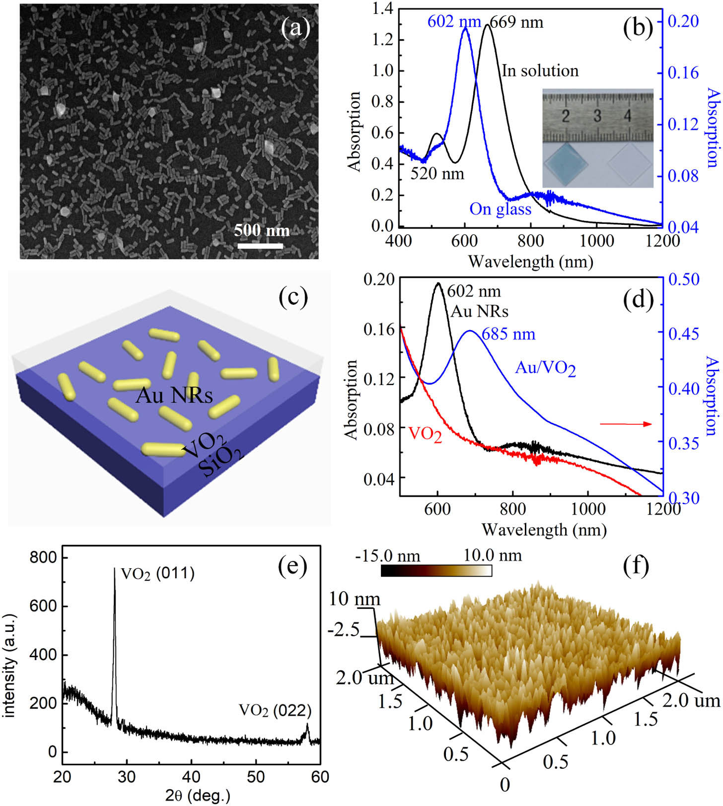
Figure 1.(a) SEM image of Au NRs on quartz substrate. (b) Experimental absorption spectra of Au NRs dispersed in solution (black, left axis) and deposited on quartz substrate (blue, right axis). The inset is the photograph of Au NRs deposited on quartz substrate (left) and one blank quartz substrate (right). (c) Schematic of Au NRs on quartz substrate coated by films. (d) The comparison of experimental absorption spectra for Au NRs (black), hybrid films (blue), and bare films (red) on quartz substrate, respectively. (e) X-ray diffraction pattern and (f) AFM 3D image of films deposited on quartz substrate.
To dynamically manipulate the plasmon resonance of Au NRs, the absorption spectra of hybrid films were studied at different temperatures (Fig. 2). For bare films [Figs. 2(a) and 2(b)], the absorptivity decreases as the temperature increases in the region of , while it increases after ; however, there are no detectable absorption features in the visible region during the heating and cooling, in which only a slight variation of absorption intensity is observed after the total phase transition ( and ). In contrast, for hybrid films [Figs. 2(c) and 2(d)], an obvious resonance peak is detected, which is blueshifted from 685 to 618 nm as the temperature increases, and vice versa. The arrows in Figs. 2(c) and 2(d) indicate the moving direction of the plasmonic peak with the change of temperature (red: heating; blue: cooling). Importantly, the plasmonic peak of Au NR arrays can be inversely tuned by 67 nm by controlling the temperature, which manipulates the phase transition of films. As a reversible phase-transition material, the films undergo the monoclinic insulating phase to the rutile metallic phase at , which consequently changes the optical constant [44,45]. Thus, the refractive index of films can be inversely tuned between and by heating and cooling in the visible and near-infrared regions [46,47].
![Experimental absorption spectra of bare VO2 and Au/VO2 films as a function of temperature. Heating [(a), (c)] and cooling [(b), (d)] on bare VO2 [(a), (b)] and Au/VO2 [(c), (d)] films. The arrows in (c) and (d) indicate the moving direction of the plasmonic peak with the change of temperature (red: heating; blue: cooling).](/Images/icon/loading.gif)
Figure 2.Experimental absorption spectra of bare and films as a function of temperature. Heating [(a), (c)] and cooling [(b), (d)] on bare [(a), (b)] and [(c), (d)] films. The arrows in (c) and (d) indicate the moving direction of the plasmonic peak with the change of temperature (red: heating; blue: cooling).
The plasmon resonance peaks are extracted and zoomed in Figs. 3(a) and 3(b), which further obviously validates the temperature variation of the LSPR mode. Figure 3(c) shows the hysteresis curve of the resonance peak as a function of temperature, and the loop indicates that the hybrid films have a potential for thermal memory. Combining Au NRs with films, we successfully demonstrate the reversible manipulation of optical properties for plasmonic arrays in the visible region. It should be noted that the films have a great effect on the LSPR modes of Au NRs; meanwhile, Au NRs also enhance the absorption intensity of films. To estimate the effect of Au NRs, we compare the absorption intensity between bare and films (the absorption intensity at 0.35 is used as the baseline). Figure 3(d) shows the temperature hysteresis curves of the absorptivity for bare films and hybrid films at 685 nm, which is the position of the resonance peak of films at the insulating phase. The variation tendency of the spectra for films is similar to that for bare films: the absorption intensity decreases with the increase in temperature and inversely increases as the temperature decreases. However, the absorptivity for films is higher than that for bare films at each temperature, as seen in Fig. 3(d). When the incident light interacts with Au NRs, the electromagnetic field of the incident light will excite the electron oscillations. Under the excitation, the Au NRs have the ability to concentrate the optical field around their surfaces. The local electric field around Au nanorods achieves the maximum under the optical pumping at plasmon resonance modes, which leads to strong light absorption of films [36,48]. The absorption intensity of films thus increases around the LSPR modes. As a result, from the absorption spectra, it is observed that the absorptivity for hybrid films is larger than that for bare around the LSPR modes.
Figure 3.(a), (b) Longitudinal plasmon resonance peak of films as a function of temperature. (c) Temperature hysteresis curves for the plasmon resonance peak of films. (d) Temperature hysteresis curves for the absorption variation (relative to the absorption intensity of 0.35) of bare and films, taken at 685 nm.
In order to investigate the effect of plasmonic nanoparticles on the phase transition of films, the Raman spectra are studied at different temperatures in bare and Au films, excited by a 532 nm laser (Fig. 4). The Raman fingerprint peaks at , , and are assigned to a series of phonon modes of the monoclinic phase [49,50]. The characteristic peaks at and correspond to the pairing and tilting motions of V cations, and the peak at is assigned to V-O bonding vibration [51–54]. The Raman peaks of films become weak and finally disappear with the increase of the temperature from room temperature (RT) to 60°C; the feature peaks are recovered when the temperature decreases to RT. These results verify that the films undergo the reversible transition between the insulating phase and the metallic phase during heating and cooling. Figures 4(a) and 4(b) show the Raman spectra of bare and films as a function of temperature under the optical pumping by a 532 nm laser with 0.2 mW. The phase transition occurs at 50°C and completes at 54°C in bare films; however, they decrease to 42°C and 48°C in films. When the laser power is increased to 0.5 mW, the phase transition temperature decreases to 32°C and 28°C for bare and films, respectively [Figs. 4(c) and 4(d)]. The results indicate that the phase transition temperature of films is smaller than that of bare under excitation by the same laser power. There are two key factors on the plasmonic enhanced phase transition of the : one is the plasmonic photothermal effect, and the other is the plasmonic enhanced light absorption [55,56]. The plasmonic photothermal effect is a result of photoexcitation in metal nanoparticles. The electrons are excited by a laser and show a non-equilibrium distribution in Au nanoparticles; a new Fermi electron distribution is then established at a higher temperature by electron–electron scattering, which leads to the electron thermalization. Consequently, the energy exchange between the electrons and lattice in the Au nanoparticles takes place by the electron–phonon coupling [57,58]. It is followed by the energy exchange between the Au nanoparticles and films through phonon–phonon coupling, which eventually improves the phase transition of films. Thus, the plasmonic arrays absorb the photons and convert some photon energy into thermal energy, which is then transferred to the films and further improves the phase transition of the films from insulating phase to metallic phase. On the other hand, the electronic transition process in films is induced by laser irradiation [27,59,60]. The excitation rate of films is enhanced by plasmonic Au nanoparticles. With a laser irradiation, the films absorb the photon energy, leading to electron transition from the ground state to an excitation state. The excitation rate is defined as , where is the transition dipole moment and is the local excitation field [56]. Thus, the excitation rate can be enhanced due to the enhanced local electric field, which also improves the lighting-induced phase transition of pristine .
Figure 4.Raman spectra of bare [(a), (c)] and [(b), (d)] films at different temperatures under optical pumping by 532 nm laser with the power of 0.2 mW [(a), (b)] and 0.5 mW [(c), (d)]. The black arrows represent the change of the temperature.
From the comparison between Figs. 4(a) and 4(c), and Figs. 4(b) and 4(d), it is observed that the temperature of the phase transition under laser excitation of 0.5 mW is lower than that excited by 0.2 mW for both bare and films. To confirm that the phase transition of films can be induced by laser irradiation, we further investigate the Raman spectra as a function of laser power for both bare and films at RT excited by 532 nm laser. Figures 5(a)–5(e) show the comparison of Raman spectra between bare and films at different laser powers. The intensity of the Raman fingerprint peaks is different between the bare and films under the same laser power. The increase of Raman signals in films compared to that of the bare under the same laser power is due to the surface enhanced Raman scattering (SERS) [Figs. 5(a) and 5(b)], while the decrease of Raman signals results from the phase transition of films [Figs. 5(c)–5(e)]. Figure 5(f) shows the Raman peak intensity as a function of the laser power. The intensity of the Raman fingerprint feature first increases to a maximum due to the increased power of 532 nm laser and then decreases for both bare and films because of the transition from insulating phase to metallic phase. The phase transition is determined by a slow, accumulated heat effect [27,61]. The photon energy of the 532 nm (2.34 eV) laser is much higher than the band gap (0.67 eV), leading to a band-to-band electronic excitation [62]. Thus, the laser-induced heating results from the electron–electron and electron–phonon coupling, which eventually triggers the phase transition of films in our experiments.
Figure 5.Raman spectra of bare and films at different power by 532 nm laser. (a)–(e) Comparison of Raman spectra between bare (black) and (red) films at 0.2, 0.4, 0.5, 0.6, and 0.7 mW, respectively. (f) The intensity of Raman peak in bare and hybrid films as a function of laser power.
We also studied the phase transition induced by lighting only with different laser powers at room temperature, further confirming the improved phase transition caused by plasmonic nanoparticles. For bare films, the intensity of the Raman feature peak at increases to the maximum at 0.6 mW and then decreases as the power further increases. However, the laser power toward the maximum of Raman feature intensity is decreased to 0.4 mW in films, and the Raman feature peak becomes weak as the laser power increases further and disappears at 0.7 mW [Fig. 5(f)]. The laser power for the phase transition of films reduces to 0.5 mW from 0.7 mW compared with bare films (28.6% lower), which confirms that the plasmonic arrays improve the phase transition process of the . The Raman signals of films are also enhanced by the plasmonic Au nanoparticles due to the enhanced local electric field [Figs. 5(a) and 5(b)] [63–66], which highlights the possibility of investigating the phase transition with more sensitivity. The Raman mapping of films at 195, 223, and at 0.6 mW more obviously demonstrates the plasmonic arrays enhanced phase transition (Fig. 6), in which the intensity of Raman peaks is strongest in bare films; however, it almost disappears in films. The Raman intensity in the spatial mapping of Raman signals in Fig. 6 is inhomogeneous, and we speculate that is due to the rough surface morphology of films, which induces the difference of absorbed light energy [Fig. 1(f)] [67,68]. The random distribution of the Au nanoparticles’ self-assembled monolayer may also contribute to the Raman intensity inhomogeneity in Figs. 6(d)–6(f).
Figure 6.Raman mapping of (a)–(c) bare and (d)–(f) films under optical pumping by 532 nm laser at 0.6 mW. (a) and (d) . (b) and (e) . (c) and (f) .
The lighting induced phase transition of is also investigated by the white light reflection spectra. Figures 7(a) and 7(b) show the white light reflection spectra of bare as a function of temperature. As the temperature increases, the reflection intensity declines, indicating that the reflection intensity is reduced when the phase transition happens, and the reduction is more distinct at short wavelengths. When the temperature is cooling down, the reflection spectra are recovered till overlapped with the reflection curve of insulator films. From the temperature hysteresis curve of the reflection intensity at 650 nm [Fig. 7(e)], it is observed that the phase transition is also reversible. Figures 7(c) and 7(d) show the white light reflection spectra of bare and Au films under excitation by 633 nm laser at room temperature. The reflection intensity decreases as the power of the 633 nm laser increases for both bare and films, which is similar to the thermal phase transition as shown in Fig. 7(a).
Figure 7.White light reflection spectra for bare and Au films. (a), (b) Bare films with the increase and decrease of temperature, respectively. (c) Bare and (d) films excited by 633 nm laser at different laser powers. (e) Temperature hysteresis curves for the reflection intensity of bare at 650 nm. (f) Comparison of reflection intensity at 650 nm in bare (black, star) and (blue, dot) films as a function of laser power.
Figure 7(f) shows the power dependence of reflection intensity of films with and without Au nanoparticles. For bare films, the phase change occurs at 7.0 mW, and the metallic phase almost completes at 21.0 mW. However, for hybrid films, it begins the phase transition at 5.0 mW and completes at 16.0 mW. Thus, the power of the phase transition for hybrid films is lower by 28.6% than that for bare films, which is consistent with the Raman results. Both Raman and white light reflection experimental results confirm the improvement of the phase transition, which is due to the plasmonic enhanced light absorption and the photothermal effect.
4. CONCLUSION
In summary, we have experimentally demonstrated the thermal modulation of plasmon resonance of macroscale Au NR plasmonic arrays in the visible region by integrating the phase-transition materials . It has been inversely tuned between 685 nm and 618 nm due to the change of the refractive index, originating from the phase transition of between the insulating and metallic phases. Besides the thermal phase transition, the phase transition of films is also induced by laser irradiation due to the laser-induced heating. The Raman and white light reflection results confirm that plasmonic arrays improve the phase change of films due to the plasmonic enhanced light absorption and the photothermal effect. A 28.6% decrease in laser power for films is observed. Our work highlights the feasibility of applying plasmonic arrays for optical modulation and plasmonic enhanced spectroscopy; the inverse tuning of the absorption resonance peak in the visible range also raises a possibility for achieving electrically driven multi-spectral imaging using one plasmonic filter.
Acknowledgment
Acknowledgment. We thank Longquan Chen and Binyu Zhao, from Southwest Jiaotong University, for providing the AFM measurement.
References
[1] N. Yu, P. Genevet, M. A. Kats, F. Aieta, J. P. Tetienne, F. Capasso, Z. Gaburro. Light propagation with phase discontinuities: generalized laws of reflection and refraction. Science, 334, 333-337(2011).
[2] X. Xu, B. Peng, D. Li, J. Zhang, L. M. Wong, Q. Zhang, S. Wang, Q. Xiong. Flexible visible-infrared metamaterials and their applications in highly sensitive chemical and biological sensing. Nano Lett., 11, 3232-3238(2011).
[3] N. Yu, F. Capasso. Flat optics with designer metasurfaces. Nat. Mater., 13, 139-150(2014).
[4] A. Arbabi, E. Arbabi, S. M. Kamali, Y. Horie, S. Han, A. Faraon. Miniature optical planar camera based on a wide-angle metasurface doublet corrected for monochromatic aberrations. Nat. Commun., 7, 13682(2016).
[5] W. Ye, F. Zeuner, X. Li, B. Reineke, S. He, C. W. Qiu, J. Liu, Y. Wang, S. Zhang, T. Zentgraf. Spin and wavelength multiplexed nonlinear metasurface holography. Nat. Commun., 7, 11930(2016).
[6] Q. Wang, E. T. F. Rogers, B. Gholipour, C.-M. Wang, G. Yuan, J. Teng, N. I. Zheludev. Optically reconfigurable metasurfaces and photonic devices based on phase change materials. Nat. Photonics, 10, 60-65(2016).
[7] L. Liu, X. Zhang, M. Kenney, X. Su, N. Xu, C. Ouyang, Y. Shi, J. Han, W. Zhang, S. Zhang. Broadband metasurfaces with simultaneous control of phase and amplitude. Adv. Mater., 26, 5031-5036(2014).
[8] E. Almeida, O. Bitton, Y. Prior. Nonlinear metamaterials for holography. Nat. Commun., 7, 12533(2016).
[9] M. R. Hashemi, S. H. Yang, T. Wang, N. Sepúlveda, M. Jarrahi. Electronically-controlled beam-steering through vanadium dioxide metasurfaces. Sci. Rep., 6, 35439(2016).
[10] C. Liu, Y. Bai, Q. Zhao, Y. Yang, H. Chen, J. Zhou, L. Qiao. Fully controllable Pancharatnam–Berry metasurface array with high conversion efficiency and broad bandwidth. Sci. Rep., 6, 34819(2016).
[11] X. Ni, A. V. Kildishev, V. M. Shalaev. Metasurface holograms for visible light. Nat. Commun., 4, 2807(2013).
[12] N. Yu, F. Aieta, P. Genevet, M. A. Kats, Z. Gaburro, F. Capasso. A broadband, background-free quarter-wave plate based on plasmonic metasurfaces. Nano Lett., 12, 6328-6333(2012).
[13] L. Kang, Y. Cui, S. Lan, S. P. Rodrigues, M. L. Brongersma, W. Cai. Electrifying photonic metamaterials for tunable nonlinear optics. Nat. Commun., 5, 4680(2014).
[14] J. Y. Ou, E. Plum, J. Zhang, N. I. Zheludev. An electromechanically reconfigurable plasmonic metamaterial operating in the near-infrared. Nat. Nanotechnol., 8, 252-255(2013).
[15] L. Huang, X. Chen, H. Mühlenbernd, G. Li, B. Bai, Q. Tan, G. Jin, T. Zentgraf, S. Zhang. Dispersionless phase discontinuities for controlling light propagation. Nano Lett., 12, 5750-5755(2012).
[16] F. Qin, L. Ding, L. Zhang, F. Monticone, C. C. Chum, J. Deng, S. Mei, Y. Li, J. Teng, M. Hong, S. Zhang, A. Alu, C. W. Qiu. Hybrid bilayer plasmonic metasurface efficiently manipulates visible light. Sci. Adv., 2, e1501168(2016).
[17] J. Shi, X. Fang, E. T. F. Rogers, E. Plum, K. F. MacDonald, N. I. Zheludev. Coherent control of Snell’s law at metasurfaces. Opt. Express, 22, 21051-21060(2014).
[18] Y. Yang, W. Wang, P. Moitra, I. I. Kravchenko, D. P. Briggs, J. Valentine. Dielectric meta-reflect array for broadband linear polarization conversion and optical vortex generation. Nano Lett., 14, 1394-1399(2014).
[19] L. Huang, X. Chen, H. Mühlenbernd, H. Zhang, S. Chen, B. Bai, Q. Tan, G. Jin, K.-W. Cheah, C.-W. Qiu, J. Li, T. Zentgraf, S. Zhang. Three-dimensional optical holography using a plasmonic metasurface. Nat. Commun., 4, 2808(2013).
[20] J. Kobashi, H. Yoshida, M. Ozaki. Planar optics with patterned chiral liquid crystals. Nat. Photonics, 10, 389-392(2016).
[21] Y. Yao, R. Shankar, M. A. Kats, Y. Song, J. Kong, M. Loncar, F. Capasso. Electrically tunable metasurface perfect absorbers for ultrathin mid-infrared optical modulators. Nano Lett., 14, 6526-6532(2014).
[22] P. Hosseini, C. D. Wright, H. Bhaskaran. An optoelectronic framework enabled by low-dimensional phase-change films. Nature, 511, 206-211(2014).
[23] J. He, Z. Xie, W. Sun, X. Wang, Y. Ji, S. Wang, Y. Lin, Y. Zhang. Terahertz tunable metasurface lens based on vanadium dioxide phase transition. Plasmonics, 11, 1285-1290(2016).
[24] J. Rensberg, S. Zhang, Y. Zhou, A. S. McLeod, C. Schwarz, M. Goldflam, M. Liu, J. Kerbusch, R. Nawrodt, S. Ramanathan, D. N. Basov, F. Capasso, C. Ronning, M. A. Kats. Active optical metasurfaces based on defect-engineered phase-transition materials. Nano Lett., 16, 1050-1055(2016).
[25] K. Appavoo, R. F. Haglund. Detecting nanoscale size dependence in VO2 phase transition using a split-ring resonator metamaterial. Nano Lett., 11, 1025-1031(2011).
[26] D. Y. Lei, K. Appavoo, F. Ligmajer, Y. Sonnefraud, R. F. Haglund, S. A. Maier. Optically-triggered nanoscale memory effect in a hybrid plasmonic-phase changing nanostructure. ACS Photon., 2, 1306-1313(2015).
[27] O. L. Muskens, L. Bergamini, Y. Wang, J. M. Gaskell, N. Zabala, C. H. de Groot, D. W. Sheel, J. Aizpurua. Antenna-assisted picosecond control of nanoscale phase transition in vanadium dioxide. Light Sci. Appl., 5, e16173(2016).
[28] D. W. Ferrara, J. Nag, E. R. MacQuarrie, A. B. Kaye, R. F. Haglund. Plasmonic probe of the semiconductor to metal phase transition in vanadium dioxide. Nano Lett., 13, 4169-4175(2013).
[29] J. Y. Suh, E. U. Donev, D. W. Ferrara, K. A. Tetz, L. C. Feldman, R. F. Haglund. Modulation of the gold particle-plasmon resonance by the metal-semiconductor transition of vanadium dioxide. J. Opt. A, 10, 055202(2008).
[30] G. Xu, Y. Chen, M. Tazawa, P. Jin. Surface plasmon resonance of silver nanoparticles on vanadium dioxide. J. Phys. Chem. B, 110, 2051-2056(2006).
[31] L. Liu, L. Kang, T. S. Mayer, D. H. Werner. Hybrid metamaterials for electrically triggered multifunctional control. Nat. Commun., 7, 13236(2016).
[32] H. Kocer, S. Butun, B. Banar, K. Wang, S. Tongay, J. Wu, K. Aydin. Thermal tuning of infrared resonant absorbers based on hybrid gold-VO2 nanostructures. Appl. Phys. Lett., 106, 161104(2015).
[33] L. Shao, Q. Ruan, R. Jiang, J. Wang. Macroscale colloidal noble metal nanocrystal arrays and their refractive index-based sensing characteristics. Small, 10, 802-811(2014).
[34] B. Peng, G. Li, D. Li, S. Dodson, Q. Zhang, J. Zhang, Y. H. Lee, H. V. Demir, X. Y. Ling, Q. Xiong. Vertically aligned gold nanorod monolayer on arbitrary substrates: self-assembly and femtomolar detection of food contaminants. ACS Nano, 7, 5993-6000(2013).
[35] H. Chen, L. Shao, Q. Li, J. Wang. Gold nanorods and their plasmonic properties. Chem. Soc. Rev., 42, 2679-2724(2013).
[36] J. Cao, T. Sun, K. T. V. Grattan. Gold nanorod-based localized surface plasmon resonance biosensors: a review. Sens. Actuators B, 195, 332-351(2014).
[37] B. M. I. van der Zande, M. R. Böhmer, L. G. J. Fokkink, C. Schönenberger. Colloidal dispersions of gold rods: synthesis and optical properties. Langmuir, 16, 451-458(2000).
[38] X. Huang, M. A. El-Sayed. Gold nanoparticles: optical properties and implementations in cancer diagnosis and photothermal therapy. J. Adv. Res., 1, 13-28(2010).
[39] S. Link, M. B. Mohamed, M. A. El-Sayed. Simulation of the optical absorption spectra of gold nanorods as a function of their aspect ratio and the effect of the medium dielectric constant. J. Phys. Chem. B, 103, 3073-3077(1999).
[40] K. M. Mayer, S. Lee, H. Liao, B. C. Rostro, A. Fuentes, P. T. Scully, C. L. Nehl, J. H. Hafner. A label-free immunoassay based upon localized surface plasmon resonance of gold nanorods. ACS Nano, 2, 687-692(2008).
[41] J. Pérez-Justea, I. Pastoriza-santos, L. Liz-Marzána, P. Mulvaney. Gold nanorods: synthesis, characterization and applications. Coord. Chem. Rev., 249, 1870-1901(2005).
[42] H. Chen, X. Kou, Z. Yang, W. Ni, J. Wang. Shape- and size-dependent refractive index sensitivity of gold nanoparticles. Langmuir, 24, 5233-5237(2008).
[43] M. Maaza, O. Nemraoui, C. Sella, A. C. Beye. Surface plasmon resonance tunability in Au-VO2 thermochromic nano-composites. Gold Bull., 38, 100-106(2005).
[44] M. J. Dicken, K. Aydin, I. M. Pryce, L. A. Sweatlock, E. M. Boyd, S. Walavalkar, J. Ma, H. A. Atwater. Frequency tunable near-infrared metamaterials based on VO2 phase transition. Opt. Express, 17, 18330-18339(2009).
[45] M. Currie, M. A. Mastro, V. D. Wheeler. Characterizing the tunable refractive index of vanadium dioxide. Opt. Mater. Express, 7, 1697-1707(2017).
[46] M. Chaker, F. Rosei. Materials research in Africa: rising from the falls. Nat. Mater., 11, 187-188(2012).
[47] H. Kakiuchida, P. Jin, S. Nakao, M. Tazawa. Optical properties of vanadium dioxide film during semiconductive-metallic phase transition. Jpn. J. Appl. Phys., 46, L113-L116(2007).
[48] M. A. García, V. Bouzas, N. Carmona. Synthesis of gold nanorods for biomedical applications. AIP Conf. Proc., 1275, 84-87(2010).
[49] P. Schilbe. Raman scattering in VO2. Physica B, 316–317, 600-602(2002).
[50] M. Pan, J. Liu, H. Zhong, S. Wang, Z. F. Li, X. Chen, W. Lu. Raman study of the phase transition in VO2 thin films. J. Cryst. Growth, 268, 178-183(2004).
[51] E. U. Donev, R. Lopez, L. C. Feldman, R. F. Haglund. Confocal Raman microscopy across the metal-insulator transition of single vanadium dioxide nanoparticles. Nano Lett., 9, 702-706(2009).
[52] D. H. Jung, H. S. So, K. H. Ko, J. W. Park, H. Lee, T. T. T. Nguyen, S. Yoon. Electrical and optical properties of VO2 thin films grown on various sapphire substrates by using RF sputtering deposition. J. Korean Phys. Soc., 69, 1787-1797(2016).
[53] H.-T. Kim, B.-G. Chae, D.-H. Youn, G. Kim, K.-Y. Kang, S.-J. Lee, K. Kim, Y.-S. Lim. Raman study of electric-field-induced first-order metal-insulator transition in VO2-based devices. Appl. Phys. Lett., 86, 242101(2005).
[54] H. Zhang, Q. Li, P. Shen, Q. Dong, B. Liu, R. Liu, T. Cui, B. Liu. The structural phase transition process of free-standing monoclinic vanadium dioxide micron-sized rods: temperature-dependent Raman study. RSC Adv., 5, 83139-83143(2015).
[55] J. Li, M. Yang, X. Sun, X. Yang, J. Xue, C. Zhu, H. Liu, Y. Xia. Micropatterning of the ferroelectric phase in a poly(vinylidene difluoride) film by plasmonic heating with gold nanocages. Angew. Chem., 128, 14032-14036(2016).
[56] B. Peng, Q. Zhang, X. Liu, Y. Ji, H. V. Demir, C. H. Huan, T. C. Sum, Q. Xiong. Fluorophore-doped core-multishell spherical plasmonic nanocavities: resonant energy transfer toward a loss compensation. ACS Nano, 6, 6250-6259(2012).
[57] S. Link, M. A. El-Sayed. Optical properties and ultrafast dynamics of metallic nanocrystals. Annu. Rev. Phys. Chem., 54, 331-366(2003).
[58] S. Link, M. A. El-Sayed. Shape and size dependence of radiative, non-radiative and photothermal properties of gold nanocrystals. Int. Rev. Phys. Chem., 19, 409-453(2000).
[59] P. Vilanova-Martínez, J. Hernández-Velasco, A. R. Landa-Cánovas, F. Agulló-Rueda. Laser heating induced phase changes of VO2 crystals in air monitored by Raman spectroscopy. J. Alloys Compd., 661, 122-125(2016).
[60] D. W. Ferrara, E. R. MacQuarrie, J. Nag, A. B. Kaye, R. F. Haglund. Plasmon-enhanced low-intensity laser switching of gold::vanadium dioxide nanocomposites. Appl. Phys. Lett., 98, 241112(2011).
[61] T. Jostmeier, J. Zimmer, H. Karl, H. J. Krenner, M. Betz. Optically imprinted reconfigurable photonic elements in a VO2 nanocomposite. Appl. Phys. Lett., 105, 071107(2014).
[62] K. Appavoo, B. Wang, N. F. Brady, M. Seo, J. Nag, R. P. Prasankumar, D. J. Hilton, S. T. Pantelides, R. F. Haglund. Ultrafast phase transition via catastrophic phonon collapse driven by plasmonic hot-electron injection. Nano Lett., 14, 1127-1133(2014).
[63] M. Yi, C. Lu, Y. Gong, Z. Qi, Y. Cui. Dual-functional sensor based on switchable plasmonic structure of VO2 nano-crystal films and Ag nanoparticles. Opt. Express, 22, 29627-29635(2014).
[64] X. Wen, Q. Zhang, J. Chai, L. M. Wong, S. Wang, Q. Xiong. Near-infrared active metamaterials and their applications in tunable surface-enhanced Raman scattering. Opt. Express, 22, 2989-2995(2014).
[65] E. U. Donev, J. I. Ziegler, R. F. Haglund, L. C. Feldman. Size effects in the structural phase transition of VO2 nanoparticles studied by surface-enhanced Raman scattering. J. Opt. A, 11, 125002(2009).
[66] B. Peng, Z. Li, E. Mutlugun, P. L. Hernández Martínez, D. Li, Q. Zhang, Y. Gao, H. V. Demir, Q. Xiong. Quantum dots on vertically aligned gold nanorod monolayer: plasmon enhanced fluorescence. Nanoscale, 6, 5592-5598(2014).
[67] R. Lopez, T. E. Haynes, L. A. Boatner. Size effects in the structural phase transition of VO2 nanoparticles. Phys. Rev. B, 65, 224113(2002).
[68] Y. Ji, Y. Zhang, M. Gao, Z. Yuan, Y. Xia, C. Jin, B. Tao, C. Chen, Q. Jia, Y. Lin. Role of microstructures on the M1-M2 phase transition in epitaxial VO2 thin films. Sci. Rep., 4, 4854(2014).


