• Photonics Research
  • Vol. 10, Issue 1, 197 (2022)
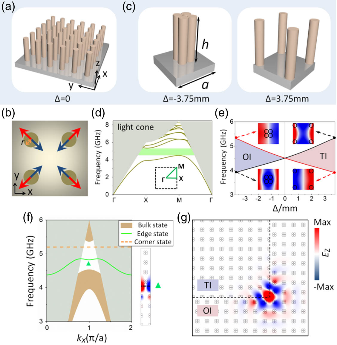
Mingxing Li1、2, Yueke Wang1、2、4、*, Tian Sang1、2、5、*, Hongchen Chu3、6、*, Yun Lai3, and Guofeng Yang1、2
Author Affiliations
  • 1Optical Information Science and Technology Department, Jiangnan University, Wuxi 214122, China
  • 2Optoelectronic Engineering and Technology Research Center, Jiangnan University, Wuxi 214122, China
  • 3National Laboratory of Solid State Microstructures, School of Physics, and Collaborative Innovation Center of Advanced Microstructures, Nanjing University, Nanjing 210093, China
  • 4e-mail: ykwang@jiangnan.edu.cn
  • 5e-mail: sangt@jiangnan.edu.cn
  • 6e-mail: chuhongchen@nju.edu.cn
  • show less
    DOI: 10.1364/PRJ.440640 Cite this Article Set citation alerts
    Mingxing Li, Yueke Wang, Tian Sang, Hongchen Chu, Yun Lai, Guofeng Yang. Experimental observation of multiple edge and corner states in photonic slabs heterostructures[J]. Photonics Research, 2022, 10(1): 197 Copy Citation Text show less
    (a) Schematic of the PCS with Δ=0. The radius and height of cylinders are r and h, respectively, and a metal plate is placed at the bottom. (b) A unit cell of PCS in (a). The blue and red arrows represent the moving direction of the cylinder. (c) 3D diagram of a unit cell with Δ=−3.75 mm (left) and Δ=3.75 mm (right); (d) band structure for PCS with Δ=±3.75 mm (inset shows the Brillouin zone). For different signs of Δ, the PCS is in a different topological phase. (e) The evolution of the lowest two bands at X point with Δ and topological phase diagram. The black and red curves represent mirror symmetric and antisymmetric modes, respectively, and the two modes are reversed at Δ=0. Insets, electric field distributions (polarized in the z direction) of the eigenstates at Δ=±3.75 mm. (f) Projected band structure for the combined PCSs of OI (Δ=−3.75 mm) and TI (Δ=3.75 mm); the green curve represents the edge state, and the orange dashed line represents the topological corner state with a frequency of 5.17 GHz in the corner structure of (g). Right inset shows the field distribution of edge state when kx=π/a (marked by the green triangle). (g) The simulated electric field distribution of the topological corner state with a frequency of 5.17 GHz; the interface of OI and TI is indicated by the black dashed lines, and a source is placed at the corner of the interface.
    Fig. 1. (a) Schematic of the PCS with Δ=0. The radius and height of cylinders are r and h, respectively, and a metal plate is placed at the bottom. (b) A unit cell of PCS in (a). The blue and red arrows represent the moving direction of the cylinder. (c) 3D diagram of a unit cell with Δ=3.75  mm (left) and Δ=3.75  mm (right); (d) band structure for PCS with Δ=±3.75  mm (inset shows the Brillouin zone). For different signs of Δ, the PCS is in a different topological phase. (e) The evolution of the lowest two bands at X point with Δ and topological phase diagram. The black and red curves represent mirror symmetric and antisymmetric modes, respectively, and the two modes are reversed at Δ=0. Insets, electric field distributions (polarized in the z direction) of the eigenstates at Δ=±3.75  mm. (f) Projected band structure for the combined PCSs of OI (Δ=3.75  mm) and TI (Δ=3.75  mm); the green curve represents the edge state, and the orange dashed line represents the topological corner state with a frequency of 5.17 GHz in the corner structure of (g). Right inset shows the field distribution of edge state when kx=π/a (marked by the green triangle). (g) The simulated electric field distribution of the topological corner state with a frequency of 5.17 GHz; the interface of OI and TI is indicated by the black dashed lines, and a source is placed at the corner of the interface.
    (a) Schematic diagram of OTO sandwiched structure. The number of TI units is denoted by N, and there are two interfaces (represented by dashed black lines) between the OI and TI domains. (b) Projected band structure of OTO PCSs with N=3 (left), 2 (middle), 1 (right); in the OTO bending structure [shown as Fig. 3(a)], the topological corner state (represented by the orange dashed line) always exists, but two CCSs (represented by blue and red dashed lines) appear only when N=1. Top insets, the field distributions of CESs marked by the blue and red triangles.
    Fig. 2. (a) Schematic diagram of OTO sandwiched structure. The number of TI units is denoted by N, and there are two interfaces (represented by dashed black lines) between the OI and TI domains. (b) Projected band structure of OTO PCSs with N=3 (left), 2 (middle), 1 (right); in the OTO bending structure [shown as Fig. 3(a)], the topological corner state (represented by the orange dashed line) always exists, but two CCSs (represented by blue and red dashed lines) appear only when N=1. Top insets, the field distributions of CESs marked by the blue and red triangles.
    (a) Photograph of the experimental OTO bending structure with N=1. The black dashed line represents the center line of the TI domain; an aluminum plate is placed at the bottom. The bottom inset shows the location of the excitation source (red star). (b) The field distribution |E|2 (EZ field distribution in the inset) of the antisymmetric CES in simulation (left panel) and experiment (right panel); the frequency of source is 4.86 GHz; (c) field distribution |E|2 (EZ field distribution in the inset) of the symmetric CES in simulation (left panel) and experiment (right panel); the frequency of source is 4.55 GHz.
    Fig. 3. (a) Photograph of the experimental OTO bending structure with N=1. The black dashed line represents the center line of the TI domain; an aluminum plate is placed at the bottom. The bottom inset shows the location of the excitation source (red star). (b) The field distribution |E|2 (EZ field distribution in the inset) of the antisymmetric CES in simulation (left panel) and experiment (right panel); the frequency of source is 4.86 GHz; (c) field distribution |E|2 (EZ field distribution in the inset) of the symmetric CES in simulation (left panel) and experiment (right panel); the frequency of source is 4.55 GHz.
    (a) Simplified schematic of the experimental OTO bend structure in Fig. 3(a). The excitation source is marked by a black dot, and the brown, blue, and red probes represent the detection of bulk, coupled edge, and corner (including topological and coupled corner) states, respectively. (b) The measured spectra for the probes at the three different positions; the frequencies of the three strongest peaks of corner spectrum are 4.66, 4.74, and 5.17 GHz. (c)–(e) The simulated (top) and experimentally measured (bottom) |E|2 and EZ (inset) field distributions of (c) antisymmetric CCS with a frequency of 4.66 GHz; (d) symmetric CCS with a frequency of 4.74 GHz; (e) topological corner state with a frequency of 5.17 GHz.
    Fig. 4. (a) Simplified schematic of the experimental OTO bend structure in Fig. 3(a). The excitation source is marked by a black dot, and the brown, blue, and red probes represent the detection of bulk, coupled edge, and corner (including topological and coupled corner) states, respectively. (b) The measured spectra for the probes at the three different positions; the frequencies of the three strongest peaks of corner spectrum are 4.66, 4.74, and 5.17 GHz. (c)–(e) The simulated (top) and experimentally measured (bottom) |E|2 and EZ (inset) field distributions of (c) antisymmetric CCS with a frequency of 4.66 GHz; (d) symmetric CCS with a frequency of 4.74 GHz; (e) topological corner state with a frequency of 5.17 GHz.
    (a), (b) Schematics of the sample with a shift of one cylinder and |E|2 field distributions of three corner states; the red cylinder moves 3 mm along the (a) y direction and (b) both the x and −y directions. (c) Schematics of the sample with a removal of cylinders and |E|2 field distributions of three corner states; the defect positions are indicated by the blue boxes.
    Fig. 5. (a), (b) Schematics of the sample with a shift of one cylinder and |E|2 field distributions of three corner states; the red cylinder moves 3 mm along the (a) y direction and (b) both the x and y directions. (c) Schematics of the sample with a removal of cylinders and |E|2 field distributions of three corner states; the defect positions are indicated by the blue boxes.
    (a) Maximal Wyckoff positions of C4-symmetric unit cell; (b) primitive generator of our topological photonic crystal.
    Fig. 6. (a) Maximal Wyckoff positions of C4-symmetric unit cell; (b) primitive generator of our topological photonic crystal.
    (a) Schematic diagram of TOT sandwiched structure; the number of OI units is denoted by M; (b)–(d) projected band diagram of TOT PCSs with (b) M=3, (c) M=2, and (d) M=1. The frequency of the topological corner state is indicated by the orange dashed line. The top insets show the field distributions EZ of the two states (red and blue curves) at kx=π/a. The simulated field distribution |E|2 of topological corner state with (e) M=2 and (f) M=1 in the OTO corner structure.
    Fig. 7. (a) Schematic diagram of TOT sandwiched structure; the number of OI units is denoted by M; (b)–(d) projected band diagram of TOT PCSs with (b) M=3, (c) M=2, and (d) M=1. The frequency of the topological corner state is indicated by the orange dashed line. The top insets show the field distributions EZ of the two states (red and blue curves) at kx=π/a. The simulated field distribution |E|2 of topological corner state with (e) M=2 and (f) M=1 in the OTO corner structure.
    (a) EZ fields of four degenerate eigenmodes of the topological corner state (around 5.17 GHz) in the box-shaped OTO structure with 22×22 periods; EZ fields of four degenerate eigenmodes of (b), (c) two CCSs (around 4.66 and 4.74 GHz) and (d) topological corner state (around 5.17 GHz) in the box-shaped OTO structure with 26×26 periods; (e) EZ fields of one eigenmode of the three corner states (with a frequency of 4.74, 4.66, and 5.17 GHz from left to right, respectively) in a larger-sized metastructure with 30×30 periods, which verifies that there is no coupling among the corners when the size is large enough.
    Fig. 8. (a) EZ fields of four degenerate eigenmodes of the topological corner state (around 5.17 GHz) in the box-shaped OTO structure with 22×22 periods; EZ fields of four degenerate eigenmodes of (b), (c) two CCSs (around 4.66 and 4.74 GHz) and (d) topological corner state (around 5.17 GHz) in the box-shaped OTO structure with 26×26 periods; (e) EZ fields of one eigenmode of the three corner states (with a frequency of 4.74, 4.66, and 5.17 GHz from left to right, respectively) in a larger-sized metastructure with 30×30 periods, which verifies that there is no coupling among the corners when the size is large enough.
    Mingxing Li, Yueke Wang, Tian Sang, Hongchen Chu, Yun Lai, Guofeng Yang. Experimental observation of multiple edge and corner states in photonic slabs heterostructures[J]. Photonics Research, 2022, 10(1): 197
    Download Citation