
Qiang PENG, Sheng-quan HE, Liang-bin REN, Xing-lian LI, Shao-ying KE. Study of Electronic Transport Characteristic and Electric Field Enhancement Effect of Wafer-bonded Si/Si p-n Junction[J]. Acta Photonica Sinica, 2020, 49(10): 1025002
- Acta Photonica Sinica
- Vol. 49, Issue 10, 1025002 (2020)
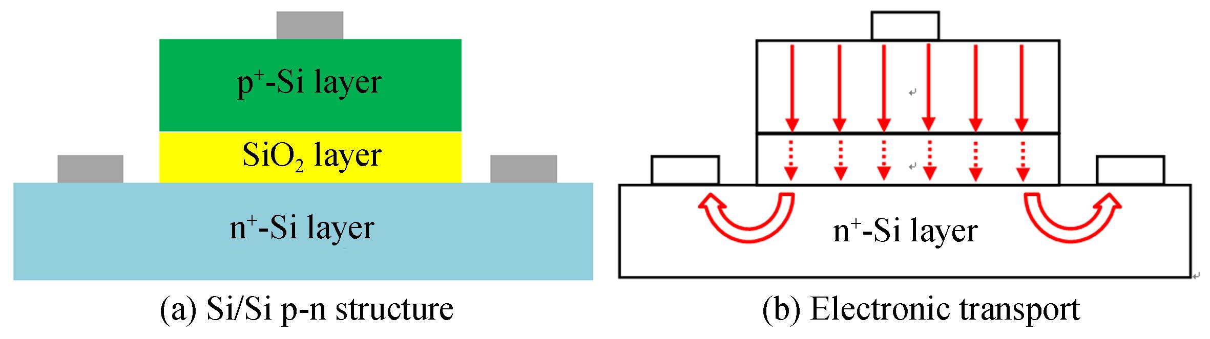
Fig. 1. Structure and electronic transport of the wafer-bonded Si/Si p-n structure
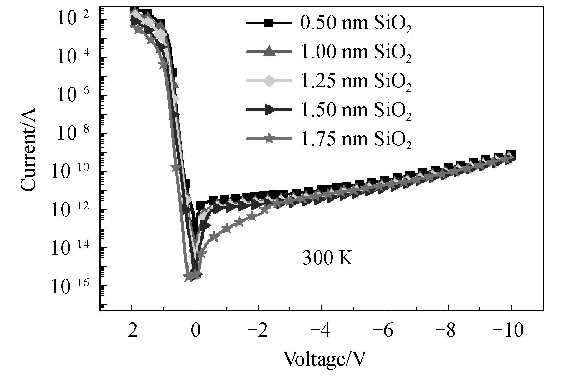
Fig. 2. Effect of d on the dark current of the Si/Si p-n junction
Fig. 3. Effect of d on the carrier tunneling rate at Si/Si bonded interface
Fig. 4. Effect of d on the recombination in the Si/Si p-n junction
Fig. 5. Effect of d on the carrier concentration in the Si/Si p-n junction (x represents the value of Y axis)
Fig. 6. Effect of d on the electric field in the Si/Si p-n junction
Fig. 7. Effect of d on the carrier velocity in the Si/Si p-n junction
Fig. 8. Effect of d on the energy band in the Si/Si p-n junction
Fig. 9. Effect of d on the charge concentration in the Si/Si p-n junction
Fig. 10. Effect of d and bias on the 3dB bandwidth of the Si/Si p-n junction
Fig. 11. Effect of the bias on the electric field in the Si/Si p-n junction
Fig. 12. Effect of the bias on the carrier velocity in the Si/Si p-n junction
Fig. 13. Effect of d on the spectrum response and total current of the Si/Si p-n junction

Set citation alerts for the article
Please enter your email address
© Copyright 2018-2021 | Chinese Laser Press. All Rights Reserved 沪ICP备15018463号-20