
Caihong Li, Wen Du, Yixuan Huang, Jihua Zou, Lingzhi Luo, Song Sun, Alexander O. Govorov, Jiang Wu, Hongxing Xu, Zhiming Wang. Photonic synapses with ultralow energy consumption for artificial visual perception and brain storage[J]. Opto-Electronic Advances, 2022, 5(9): 210069
- Opto-Electronic Advances
- Vol. 5, Issue 9, 210069 (2022)
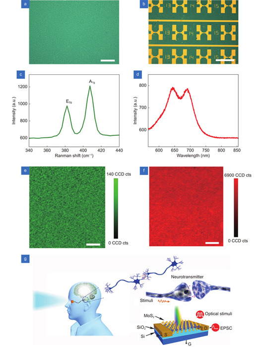
Fig. 1. Optical characterizations of MoS2 synaptic transistors and schematic diagram of human eyes. (a ) The optical image of large-area and uniform polycrystalline MoS2. Scale bar: 100 μm. (b ) The optical photograph of a MoS2 synaptic transistor array on Si/SiO2 substrate. Scale bar: 500 μm. The corrsponding Raman spectrum (c ) and PL spectrum (d ) of MoS2. The corresponding Raman mapping around 381.4 cm–1 (e ) and PL mapping (f ) selected randomly from (a). Scale bar: 8 μm. (g ) Schematic diagram of visual perception and information transmission in human brain and corresponding artifical MoS2 synaptic device.
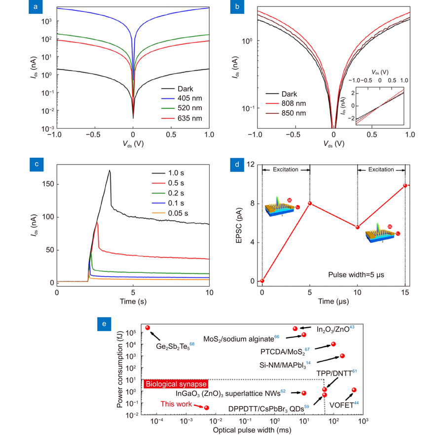
Fig. 2. Photodetection and spike-duration plasticity of the MoS2 synaptic transistor. Output characteristic curves of the MoS2 synaptic transistor in visible light (a ) and NIR light (b ). The inset in (b) is the corresponding linear output characteristic curve. (c ) The transient current responses triggered by several optical stimulus with different duration of a single pulse, respectively. (d ) The EPSC at the pulse width of 5 μs (405 nm, Vds = 1 V). (e ) Comparison of single optical pulse width and power consumption among some synaptic devices.
Fig. 3. STP characteristics of the MoS2 synaptic transistor. (a ) The transient current response induced by an optical pulse of 50 ms. (b ) The EPSC curves under different laser power densities (pulse width: 100 ms). Inset: The dependence of EPSC with differnent laser power densities (P). (c ) The instantaneous current responses triggered by a pair of optical pulses (pulse width = 50 ms, pulse interval Δt = 2 s). The black dashed line represents the initial current in (a) and (c) without optical stimuli. (d ) The PPF behaviors at different Δt.
Fig. 4. LTP characteristics of the MoS2 synaptic transistor. The transient current (a ), EPSC (b ) and the extracted forgetting curve (c ) from (a) after 10, 25, 50, 75 and 100 optical pulses. The transient current (d ), A30/A1 (e ) and the extracted forgetting curve (f ) from (d) triggered by different spike frequency where A30 means the thirtieth EPSC. The black dashed line represents the initial current in (c) and (f) without optical stimuli.
Fig. 5. Schematic illustration of the Pavlovian conditioning and emotional effect on the MoS2 synaptic transistor. The classical Pavlovian conditioning under one training (E+L) (a ) and ten trainings (b ). (c ) The transient current triggered by 30 optical spikes at the backgate of 0.1 V, 0 V and –0.1 V. (d ) The maximum EPSC at different Vg.
Fig. 6. Neuromorphic imaging simulation. (a ) Illustration of neuromorphic letter recognition. The stimulated letter recognition under STP (b ), LTP with (c ) or without (d ) -Vg.

Set citation alerts for the article
Please enter your email address
© Copyright 2018-2021 | Chinese Laser Press. All Rights Reserved 沪ICP备15018463号-20