Abstract
The human visual system, dependent on retinal cells, can be regarded as a complex combination of optical system and nervous system. Artificial retinal system could mimic the sensing and processing function of human eyes. Optically stimulated synaptic devices could serve as the building blocks for artificial retinas and subsequent information transmission system to brain. Herein, photonic synaptic transistors based on polycrystalline MoS2, which could simulate human visual perception and brain storage, are presented. Moreover, the photodetection range from visible light to near-infrared light of MoS2 multilayer could extend human eyes’ vision limitation to near-infrared light. Additionally, the photonic synaptic transistor shows an ultrafast speed within 5 μs and ultralow power consumption under optical stimuli about 40 aJ, several orders of magnitude lower than biological synapses (50 ms and 10 fJ). Furthermore, the backgate control could act as emotional modulation of the artificial brain to enhance or suppress memory function, i.e. the intensity of photoresponse. The proposed carrier trapping/detrapping as the main working mechanism is presented for the device. In addition, synaptic functionalities including short synaptic plasticity, long synaptic plasticity and paired-pulse facilitation could be successfully simulated based on the prepared device. Furthermore, the large difference between short synaptic plasticity and long synaptic plasticity reveals the better image pre-processing function of the prepared photonic synapses. The classical Pavlovian conditioning associated with the associative learning is successfully implemented as well. Therefore, the efficient and rich functionalities demonstrate the potential of the MoS2 synaptic device that integrates sensing-memory-preprocessing capabilities for realizing artificial neural networks with different emotions that mimic human retina and brain.The human visual system, dependent on retinal cells, can be regarded as a complex combination of optical system and nervous system. Artificial retinal system could mimic the sensing and processing function of human eyes. Optically stimulated synaptic devices could serve as the building blocks for artificial retinas and subsequent information transmission system to brain. Herein, photonic synaptic transistors based on polycrystalline MoS2, which could simulate human visual perception and brain storage, are presented. Moreover, the photodetection range from visible light to near-infrared light of MoS2 multilayer could extend human eyes’ vision limitation to near-infrared light. Additionally, the photonic synaptic transistor shows an ultrafast speed within 5 μs and ultralow power consumption under optical stimuli about 40 aJ, several orders of magnitude lower than biological synapses (50 ms and 10 fJ). Furthermore, the backgate control could act as emotional modulation of the artificial brain to enhance or suppress memory function, i.e. the intensity of photoresponse. The proposed carrier trapping/detrapping as the main working mechanism is presented for the device. In addition, synaptic functionalities including short synaptic plasticity, long synaptic plasticity and paired-pulse facilitation could be successfully simulated based on the prepared device. Furthermore, the large difference between short synaptic plasticity and long synaptic plasticity reveals the better image pre-processing function of the prepared photonic synapses. The classical Pavlovian conditioning associated with the associative learning is successfully implemented as well. Therefore, the efficient and rich functionalities demonstrate the potential of the MoS2 synaptic device that integrates sensing-memory-preprocessing capabilities for realizing artificial neural networks with different emotions that mimic human retina and brain.Introduction
Researches on artificial neural networks (ANN) which could offer both storage and computing have been carried out extensively in order to obtain a deeper understanding of human vision and brain1, 2. For example, synaptic transistors, memristors3, phase change memories, etc. have been widely applied to simulate biological neurons4-6. Furthermore, the spiking neural networks (SNN), as the third generation of ANN, are the biologically-realistic models of living nervous systems taking discrete events instead of continuous values as stimuli7. From a single device to an array of devices, increased number of more complex functions could be realized, such as the field of artificial intelligence (AI) related to vision8-11. In addition, associative learning based on the interaction between thoughts and experience is one of the most important capabilities of human brain cells12. The classical Pavlovian conditioning links two stimuli together to produce a new learned response in a person or animal13. Recently, different materials and various structures are used to stimulate the effective performance of biological synapses1, 14, 15. The main significant figure of merit are sensitivity and power consumption for evaluating neural devices16. The ideal synaptic transistors have strong synaptic plasticity and lower power consumption than bio-synapses which consumes about 10 fJ per spike1, 17, 18. Synaptic plasticity is divided into long-term synaptic plasticity (LTP) closely related to learning and memory and short-term synaptic plasticity (STP) processing the temporal information on the relevant time scales such as milliseconds or seconds12, 17. According to Hebbian theory, also called spike timing-dependent plasticity (STDP), persistent or repeated stimuli give rise to a higher synaptic weight which represents the strength of connection between two nodes19-21. In addition, spike-duration dependent plasticity, spike-number dependent plasticity, spike-frequency dependent plasticity, learning-experience behavior and forgetting behavior are also important parameters to measure the properties of synaptic devices17, 22.
Photonic synapses, coupling optical sensing and synaptic plasticity, are expected to reduce power consumption and achieve ultrafast signal transmission23, 24. The light-sensitive photosensors are similar to the photoreceptors of biological retina because they both can convert light signals to electrical signals25. This kind of devices, which could mimic the biologic eyes and work as a standalone platform, would pave the way for machine vision systems in the future26. Moreover, Lee’s group have extended the human visual sense beyond visible light to UV light and this work may be further applied to healthcare via combining UV selectivity and dose-calculation27.
Optical modulation as a novel gate-control mode for achieving multi-terminal neuromodulations could decrease thermal loss and operate simply17. The light-stimulated synaptic device offers more possibilities to broaden the functionalities and system complexities of the current neuromorphic systems24. Two-dimensional (2D) transition metal dichalcogenides (TMDs) are intriguing and promising optoelectronic devices due to their superb electrical and optical properties28, 29. Many kinds of 2D TMDs could be synthesized in large-area by chemical vapor deposition (CVD) or other methods, making practical devices possible30-34. Molybdenum disulfide (MoS2) has been investigated as an efficient charge-trapping layer and light absorption layer in photonic synapses recently due to fast charge-trapping rate, good trapped charge-retention, good optical absorption35, 36 and high carrier mobilities1, 17, 18, 37, 38. Yoo’s group37 has confirmed that the MoS2 layer could act as a high-efficiency charge-trapping layer via control experiment. Although the two-terminal devices are easier to form a crossbar-array structure, the inhibitory synaptic behaviours cannot be achieved in these devices39. Furthermore, three-terminal gate-control synaptic transistors are able to possess another degree-of-freedom to modulate the neuromorphic function apart from optical modulation8, 40. For instance, Chu’s group40 have shown a gate tunable artificial synapse to mimic the modulation of drug dosage. In addition, MoS2 with intrinsic flexibility could be applied to curved image sensor array for the machine vision41.
The proposed mechanism for photonic synapses is charge trapping/detrapping or phase change5, 39. The former could achieve low-energy consumption instead of the requirement of high power supplies for the latter39. In addition, the trap centers capturing and releasing carriers could be material defects, surface dangling bonds, potential wells35, etc42. The persistent photocurrent/photoconductivity caused by these trap centers make the device be able to mimic some specific functions of biological synapses26. Given that, the TMDs with outstanding photoelectric conversion properties and various defects as carrier traps show great potential acting as optically active layers for photonic synapses39. Additionally, the von Neumann bottleneck caused by separated memory units and processing makes synaptic devices with low power consumption more desired43. However, electrical synapses under low-energy consumption17 could be achieved via ultrashort electrical pulses while the photonic synapses with ultralow power consumption to attojoule (aJ) level are still few, especially via ultrashort optical pulses44.
In this work, the large-area growth 2D MoS2 films and an array of MoS2 synaptic transistors integrating the sensing-memory-preprocessing capabilities are demonstrated. The photosensing scope of our devices broadens humanoid vision to near-infrared light. Moreover, the photonic synapses under visible light possess hypersensitivity to transient single pulse and ultralow power consumption superior to bio-synapses. Specifically, the synaptic plasticity via photoinduced charge transfer is investigated including STP, LTP, paired-pulse facilitation (PPF) and the forgetting behavior23. The classical Pavlovian conditioning can also be verified by our synaptic device. In addition, back-gate bias could enhance or reduce memory function exhibiting similar effects of emotions25. Positive emotions offer a positive effect and vice versa. The image pre-processing is achieved by the large contrast between STP and LTP. Given that, we can conclude such synaptic devices are promising building blocks in AI, especially visual perception and brain storage26, 27, 45.
Results and discussion
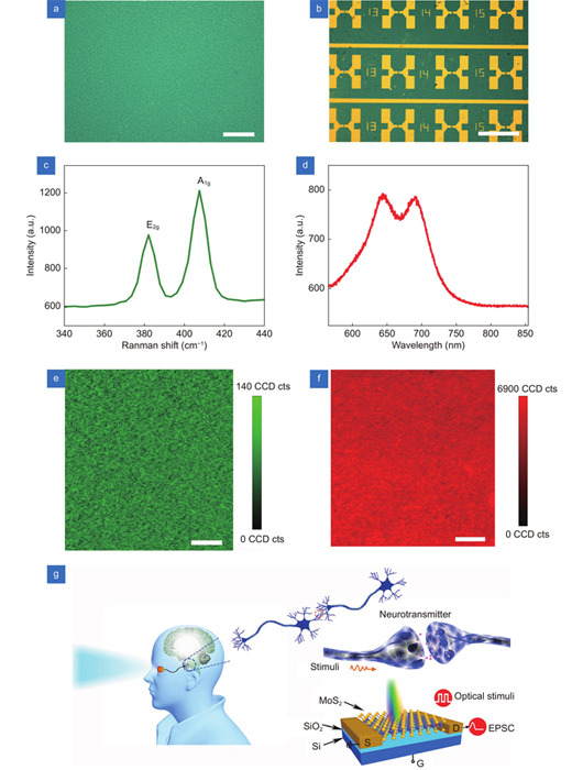
Synapses, i.e. neuronal junction, could transmit electric nerve impulses between neurons and effectors to achieve signal transmission17. In order to mimic the properties of synapses, MoS2 synaptic transistors are prepared via low pressure CVD (LPCVD) for improved thickness uniformity34. The details of material growth and device fabrication are presented in the Experimental section. The accurate control of material growth condition including pressure, temperature, the amount of precursors, the position of substrates and so on could improve the reproducibility of channel material. The optical image of the polycrystalline MoS2 film on a Si/SiO2 substrate is shown in Fig. 1(a). A continuous and relatively uniform large-area film over 2 cm2 is grown successfully. Figure 1(b) shows the optical microscopy image of a part of the MoS2 synaptic transistor array. The devices are fabricated by standard lithography with Ti/Au electrodes as the source, drain, and silicon as the backgate. The corresponding Raman spectrum in Fig. 1(c) shows the typical E2g (381.9 cm–1) and A1g (407.3 cm–1) peaks of MoS2 measured by the 532 nm laser28, 33, 46. The frequency difference between E2g and A1g is about 25.4 cm–1 indicating multilayer growth, which was further confirmed by PL spectrum47 in Fig. 1(d). Figure 1(e) and 1(f) show the corresponding Raman mapping around 381.4 cm–1 and PL mapping selected randomly from Fig. 1(a). The material uniformity of as-grown MoS2 films can be further confirmed by the uniform color contrast of Raman and PL signals in Fig. 1(e) and 1(f)48. Figure 1(g) shows a schematic of the visual perception of human eyes and information transmission to the brain based on our MoS2 synaptic transistors. The retina in human eyes could detect the visible light and then transmit the information to brain via a number of synapses27. Under external stimuli such as optical and electrical pulse, the source and drain electrodes are used to liken pre- and post-synaptic terminals, respectively25. Additionally, gate modulation can serve as another form of signal input for three-terminal artificial synapses8, 40.

Figure 1.Optical characterizations of MoS2 synaptic transistors and schematic diagram of human eyes. (a) The optical image of large-area and uniform polycrystalline MoS2. Scale bar: 100 μm. (b) The optical photograph of a MoS2 synaptic transistor array on Si/SiO2 substrate. Scale bar: 500 μm. The corrsponding Raman spectrum (c) and PL spectrum (d) of MoS2. The corresponding Raman mapping around 381.4 cm–1 (e) and PL mapping (f) selected randomly from (a). Scale bar: 8 μm. (g) Schematic diagram of visual perception and information transmission in human brain and corresponding artifical MoS2 synaptic device.
Photonic synapses which integrate sensing and synaptic function could mimic the visual perception of human retina27. The bias voltage (Vds) of 1 V was applied for the following measurements without special instructions. The visible light detection is depicted in Fig. 2(a) and three different wavelengths are chosen including 405 nm, 520 nm and 635 nm. Surprisingly, near-infrared (NIR) light such as 808 nm and 850 nm could also be detected without the upconverting nanoparticles mediation which could upconvert NIR to visible light or UV18 shown in Fig. 2(b). Because multilayer MoS2 photodetectors could be responsive to NIR light while monolayer MoS2 ones could only detect visible light49, 50. This reveals the capability of photoreception of our device could be extended to NIR as human eyes could only detect the visible light. The broadband detection from visible to NIR light51 at room temperature based on our MoS2 synaptic transistors provides new opportunities in machine vision. The insert in Fig. 2(b) shows a good ohmic contact due to linear output characteristics between metal electrodes and MoS214, 52-56. Taking 405 nm laser as an example, synaptic function-related measurements are investigated. Figure 2(c) displays the excitatory post‐synaptic current (EPSC, i.e.
) of the synaptic device under different single pulse width, showing the spike-duration plasticity17. According to Fig. 2(c), the MoS2 transistor shows typical synaptic properties, i.e. the effects after stimuli do not disappear immediately with the disappearance of the stimuli. The proposed working mechanism based on our photonic synapses is that the charge trapping centers provided by the channel and interfaces reserve the photoinduced carriers even after removing the optical stimuli57. That is to say, the persistent photocurrent/photoconductivity phenomenon is attributed to slow recombination of defect or trap centers35. The building potential wells between MoS2 and source-drain electrodes could reserve/release charge carriers with the modulation of light stimuli35. The trap sites in the potential wells may originate from the sulfur vacancies in the channel and the dangling Si-O bonds at the interface of MoS2/SiO235. The proposed operating process of our photonic synapses might be the state of thermal equilibrium without optical/electrical stimuli at the beginning and generation of photocarrier under optical stimuli followed by carrier trapping, carrier recombination and returning to the original state under dark43. In addition, the photocurrent will enhance as the single pulse width prolong obtained from Fig. 2(c) due to the production of more photogenerated carriers. Furthermore, the synaptic transistor distinctly responds to a very short optical pulse with a width of only 5 μs in Fig. 2(d) which is four orders of magnitude faster than the instantaneous information transmission in the biological synapses (typically 50 ms)58. Possible reasons for the ultrashort optical pulse detection capability are ultrafast optical signal propagation speed2, 35, 39, 59 and ultrasensitive optical detection60 based on the polycrystalline MoS2 films. As a result, our synaptic transistors could improve the recognition rate of single optical pulse significantly and achieve an ultralow power consumption of 40 aJ, two orders of magnitude lower than that of biological synapses. The power consumption of one synaptic event could be estimated by the equation of
where Ipeak, Vread and t are the maximum EPSC after a pulse, reading voltage and pulse width, respectively6. Our power consumption could be reduced by shortening the pulse width with constant reading voltage of 1 V, while many researches achieve low power consumption via decreasing the reading voltage44, 59, 61, 62 such as 10 μV. So far, the minimum power consumption of a single optical pulse is about femtojoule (fJ) level, well above that of ours (Fig. 2(e))5, 14, 17, 42-44, 59, 61-68. The ultralow power consumption and ultrafast speed suggest the prepared device a promising candidate for an energy-efficient neuromorphic computing system17.
Figure 2.Photodetection and spike-duration plasticity of the MoS2 synaptic transistor. Output characteristic curves of the MoS2 synaptic transistor in visible light (a) and NIR light (b). The inset in (b) is the corresponding linear output characteristic curve. (c) The transient current responses triggered by several optical stimulus with different duration of a single pulse, respectively. (d) The EPSC at the pulse width of 5 μs (405 nm, Vds = 1 V). (e) Comparison of single optical pulse width and power consumption among some synaptic devices.
STP, also called short-term memory (STM), is a critical source information for associative learning and sound localization like classical Pavlovian conditioning12. Figure 3(a) shows a clear and typical synaptic response at a single pulse width of 50 ms like the information transmission speed in biological synapses69 and Vds of 1 V. This optical pulse (405 nm) results in an acute current rise due to a sudden increase of photoinduced carriers70. After the optical pulse is off, the EPSC exhibits a slow delay and relatively long relaxation time because the trapped holes by the surface states caused a low recombination rate of carriers12, 70. Figure 3(b) and inset unfold the EPSC would enhance as the power density (P) of the single optical pulse (width: 100 ms). At the higher P, the faster decay time can be observed in Fig. 3(b) because the decay dynamics are dominated by shallow carrier traps rather than deep carrier traps at lower P71. Additionally, the sublinear relationship between EPSC and P in the inset of Fig.3(b) confirmed the presence of trap states further72. The sublinear relationship is attributed to the photogating effect73 caused by long-lived charge trapping processes71. The PPF triggered by two consecutive presynaptic spikes at 2 s intervals is expressed in Fig. 3(c). A higher EPSC would be obtained after the second optical spike because of the effect of the first optical spike. The PPF index is defined as the ratio of A2 to A1 where A2 and A1 mean the EPSC triggered by the second or first light spike, respectively18, 74. Figure 3(d) shows the PPF index increases as the pulse interval (Δt) decreases. This is in accordance with the behaviour of information processing in biological synapses14. Furthermore, the characteristic relaxation times of rapid and slow decay constants τ1and τ2 can be estimated according to the double-exponential decay function given by
Eq. (1)18, 75.
![]()
![]()
where C0 equals to 1, which indicates the trend of PPF index is towards to 100% eventually67. In our case, the values of τ1 and τ2 are 0.8 s and 9.2 s fitted from Fig.3(d), respectively. Additionally, the age-related learning characteristics could be emulated by our synaptic transistors thanks to the PPF characteristics which are varied with human age76.
Figure 3.STP characteristics of the MoS2 synaptic transistor. (a) The transient current response induced by an optical pulse of 50 ms. (b) The EPSC curves under different laser power densities (pulse width: 100 ms). Inset: The dependence of EPSC with differnent laser power densities (P). (c) The instantaneous current responses triggered by a pair of optical pulses (pulse width = 50 ms, pulse interval Δt = 2 s). The black dashed line represents the initial current in (a) and (c) without optical stimuli. (d) The PPF behaviors at different Δt.
Compared with STP, the LTP, i.e. long-term memory (LTM), usually takes longer time which means the lasting potentiation of the synaptic weight12. Figure 4(a–c) show the spike-number dependent LTP and forgetting behavior. The number of spikes could be regarded as the learning times70. There is a continuous upward trend of current as the number of spikes increases due to more and more photoinduced carriers. This is similar to biological synapses because successive stimuli could induce more neurotransmitters6. This phonomenon could explain more and more high-efficiency relearning behavior of a human’s brain39. The forgetting behavior is liken by the EPSC after the optical spikes14. At first, the forgetting behavior would decrease rapidly and then decay slowly which is coincident with human brain22, 70. As seen in Fig. 4(c), the delay of the transient current after photostimulation is fast at the beginning and then becomes slow. The delay speed is dependent on three continuous stages including recombination, shallow and deep trapping procedures77. The defect-induced recombination and traps make the corresponding fast and slow delay78. In addition, the spike-frequency dependent LTP and forgetting behavior are shown in Fig. 4(d–f). The higher frequency of repeated stimuli could enhance the synaptic weight and improve the memory function or learning efficiency obtained from Fig. 4(d)17, 76. Moreover, the MoS2 synaptic transistor shows the characteristic of the biological high-pass filters which could be applied for filtering unnecessary information in signal processing as shown in Fig. 4(e)6, 14, 26, 70. The EPSC would become saturated eventually even though the number or frequency of optical pulses increases continuously. This means the synaptic device would not cause excessive neural activity6. From Fig. 4(c) and 4(f), the forgetting processes follow the classical Ebbinghaus forgetting curve which indicates the memory decays over time79-81. Furthermore, the higher-learning condition stimulated by more spike numbers or higher spike frequency leads to slower forgetting82. Note that the effect of single pulse duration time on synaptic plasticity is similar to spike number and the same is true for the Δt between two continuous stimuli and spike frequency9.
Figure 4.LTP characteristics of the MoS2 synaptic transistor. The transient current (a), EPSC (b) and the extracted forgetting curve (c) from (a) after 10, 25, 50, 75 and 100 optical pulses. The transient current (d), A30/A1 (e) and the extracted forgetting curve (f) from (d) triggered by different spike frequency where A30 means the thirtieth EPSC. The black dashed line represents the initial current in (c) and (f) without optical stimuli.
The Pavlovian conditioning, as unconscious or procedural memory, could help creatures to be prepared for something expected or likely13. This process, a classical example of the associative learning, is consist of the acquisition, extinction and recovery12. The artificial synaptic devices could remember their past dynamic history, which is vital to mimic the Pavlovian conditioning12, 13. Figure 5(a) shows the typical Pavlovian conditioning under one training. Here, the electrical spikes (E) of Vds and light spikes (L) act as the bell and bones in the Pavlov’s dog experiment. The bell ringing would make the dog salivate after the training of feeding and ringing bells together13. In Fig. 5(a) and 5(b), the black dashed line represents the threshold value of salivation. The EPSC under E would not reach the threshold value initially. However, the later E could induce salivation for the next five minutes after the stimuli of E and L together (E + L) shown in Fig. 5(a). In addition, 10 successive E + L spikes are applied as repeated trainings in Fig. 5(b). The EPSC maximum is far more than the threshold value after 10 spikes and the salivation state would last at least half an hour. This means the classical Pavlovian conditioning could be mimicked successfully based on our MoS2 synaptic device and more trainings could make better associative learning.
Figure 5.Schematic illustration of the Pavlovian conditioning and emotional effect on the MoS2 synaptic transistor. The classical Pavlovian conditioning under one training (E+L) (a) and ten trainings (b). (c) The transient current triggered by 30 optical spikes at the backgate of 0.1 V, 0 V and –0.1 V. (d) The maximum EPSC at different Vg.
The backgate (Vg) could regulate the memory function of our synaptic device as well except for repeated optical stimuli or electrical stimuli of Vds4, 14, 18, 83. Figure 5(c) and 5(d) depict the memory function of the synaptic transistor could be modulated by changing the Vg simply. It functions like the emotional effect on the memory function of human brain84, 85. Figure 5(c) shows the small negative Vg of –0.1 V could significantly enhance the transient current under 30 optical spikes than that at zero gate voltage. On the contrary, the positive Vg could make the transient current decrease drastically. This phenomenon of increased EPSC may be attributed to negative gate voltage assisted detrapping of electrons. Cheng’s group has reported that the free electron concentration or channel conductance increased due to released trapped electrons after negative gate voltage86. On the contrary, the positive gate voltage would make the free eletrons in the channel easier be trapped by trap centers resulting in the reduced channel conductance86. The inhibited current increment due to the applied positive gate voltage does not equate to the conventional inhibitory post-synaptic current24, 87. The carrier trapping/detrapping under different positive/negative gate voltage is considered as the main operation mechanism of current switching behavior for the three-terminal artificial synapses1, 35, 57. The negative Vg could act like the positive emotions, and vice versa when positive Vg for our device. It is well-known that someone could have a better memory function in a good mood. A more obvious gate-tunable phenomenon is shown in Fig. 5(d). The EPSC would increase to about five times at the Vg of –1 V than that without Vg. Thus, our synaptic device could be applied for mimicking the visual learning and memory process at different emotions.
Inspired by human retina, our synaptic device would be further applied for neuromorphic imaging and pre-processing due to the excellent light-stimulated synaptic properties and easy large-area growth41. Figure 6(a) shows the schematic diagram of human’s neuromorphic visual system. Given that, we stimulate the letter recognition of “I” under STP, LTP with or without -Vg shown in Fig. 6(b–d). The time needed for photocurrent decay to 1/e of its original state are 40 s and 2 min, respectively, for STP and LTP at zero Vg obtained from Fig. 6(b) and 6(c). The retention time of LTP is much longer than that of STP. The difference between LTP and STP is resulted from the different photo dosage which can make different effect on device conductance and decay dynamics35. When the −Vg was applied on the synaptic device, the photocurrent improved significantly in Fig. 6(d). Additionally, the big difference between STP and LTP makes the MoS2 synaptic device show a better contrast in the pre-processing which is very important for efficient machine vision15, 41.
Figure 6.Neuromorphic imaging simulation. (a) Illustration of neuromorphic letter recognition. The stimulated letter recognition under STP (b), LTP with (c) or without (d) -Vg.
Conclusions
In summary, the uniform polycrystalline MoS2 film could be a promising choice to mimic the visual perception and brain storage. The unique charge-trapping characteristics and facile synthesis of MoS2 make it a favored candidate over other materials for bio-mimicking devices1, 17, 18, 37. The photoreception capability of our device could expand the edge of vision from visible light to NIR light. Our photonic synapses could achieve information transfer and storage of the artificial brain with sensitive response to ultrashort optical pulses and the lowest power consumption under optical stimuli reported so far. The synaptic plasticity such as STP, PPF, LTP, forgetting behavior and associative learning are successful stimulated based on this proposed device. Moreover, the emotional effect on memory by regulating the backgate voltage is demonstrated. The channel conductance modulation is achieved by carrier trapping/detrapping in the channal and interfaces/surfaces1. Eventually, like the neuromorphic imaging and pre-processing device, the prospective imaging effect is shown. This work which integrates sensing-memory-preprocessing capabilities provides an insight into artificial retinal system and artificial brain.
Experimental section
CVD growth of MoS2
The polycrystalline MoS2 was grown in a 1 in. quartz tube with a one-zone furnace. Mixed MoO3 powder (8.7 mg) and NaCl (1.4 mg) together placed in the center of the furnace and S powder (255 mg) were used as the precursor for the MoS2 growth. A pair of Si/SiO2 substrates are placed face to face with the vertical distance about 2 mm in the downstream after rinsing by acetone and isopropanol. The whole CVD process is controlled at a low pressure of 0.4 Torr (1 Torr=133.3223684 Pa) with the Ar/H2 (8∶1) as the carrier gas after purging out the air in the tube about 10 min. The S powder is ramped up to 220 °C using a heating belt when the temperature of the furnace center reaching 670 °C. Then, the furnace was maintained for 30 min when it was heated up to 750 °C. Finally, the tube was cooled to room temperature naturally after removing the furnace.
Device fabrication
The Ti/Au (Ti: 10 nm, Au: 100 nm) metals were deposited by electron beam evaporation and then lifted off in acetone as the source and drain electrodes after the photolithography.
Material characterization
The optical images were captured by OLYMPUS microscope (LV100ND). The Raman and PL data were measured with a Raman-AFM confocal spectrometer (Witec, alpha300 RA) with a laser of 532 nm.
Device characterization
The optoelectronic properties of the photonic synapses were measured with the SemiProbe probe station and a semiconductor parameter analyzer (Keithley 4200) and Platform Design Automation (PDA, FS- Pro). Different duration of optical stimuli and different laser densities set by a Programmable DC Power Supply (Itech Electronic, IT6100B), a function generator and an irradiatometer were used to measure the photoresponse.
References
[20] Hebb DO. TheOrganizationofBehavior: ANeuropsychologicalTheory (Psychology Press, London, 2005).
[21] Bear MF, Connors BW, Paradiso MA. NeuroscienceExploringtheBrain (Lippincott Williams & Wilkins, Philadelphia, 2007).
[47] Ganger ZD. Growth of two-dimensional molybdenum disulfide via chemical vapor deposition (Wright State University, Dayton, 2019).
[79] Ebbinghaus H. ÜberdasGedächtnis: UntersuchungenzurExperimentellenPsychologie (Duncker & Humber, Leipzig, 1885).