
Yingli Ha, Yu Luo, Mingbo Pu, Fei Zhang, Qiong He, Jinjin Jin, Mingfeng Xu, Yinghui Guo, Xiaogang Li, Xiong Li, Xiaoliang Ma, Xiangang Luo. Physics-data-driven intelligent optimization for large-aperture metalenses[J]. Opto-Electronic Advances, 2023, 6(11): 230133
- Opto-Electronic Advances
- Vol. 6, Issue 11, 230133 (2023)
Abstract
Introduction
In the past decade, meta-devices have shown remarkable advantages of lightweight, high integration, and high flexibility capabilities
| a)Absolute focusing efficiency; b)Relative focusing efficiency; c)Relative focusing efficiency compared to the ideal efficiency; d)Simulated result; e)Experimental result; f)Predict result | ||||||||
| Liang et al. | 532 | TiO2 | 0.98 | - | 2D | 67%a),e) | Hybrid optimization algorithm | - |
| Cai et al. | 532 | TiO2 | 0.51 | 24 | 1D | 60%a),e) | Genetic algorithm | 1000 s |
| Mansouree et al. | 850 | a-Si | 0.78 | 52 | 2D | 65%a),e) | Adjoint optimization | 97 min /iteration |
| Li et al. | RGB | TiO2 | 0.3 | 10000 | 2D | 15%a),e) | Conservative convex separable approximation | few hours |
| An et al. | 1550 | p-Si | 0.72 | 32 | 1D | 77.62%b),d) | Deep learning | 200 s |
| Phan et al. | 640 | SOI | 0.5 | 200 | 1D | 89%c),e) | Topology optimization | 100 h |
| Pestourie et al. | RGB | TiO2 | 0.3 | 235 | 1D | - | “Locally periodic” approximation | 250 s |
| Arbabi et al. | 1550 | a-Si | 0.37 | 50 | 2D | 82%a),e) | High- contrast gratings | - |
Table 1. Examples to show the representative parameters and performance of various methods.
Inverse design methods could iteratively update the real vectorial electric field for each pixel, gradually approaching the ideal electric field distribution, and can effectively solve the problems of the traditional design method
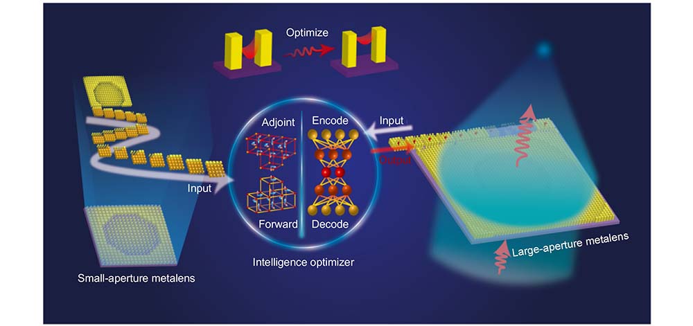
In this study, we propose a physics-data-driven design method that integrates a multi-objective optimization algorithm with a DL approach. We have developed an “intelligent optimizer” that utilizes an end-to-end design framework to achieve optimized design of large-aperture metalenses. Compared with physics-driven or data-driven optimization methods, our method has the advantages of simple network models (16 layers of neurons), low data-set requirements (~5000 data-sets), and short optimization time (6 min and 45 s@1 mm2, 2 h and 54 min@1 cm2). The simulation results provide evidence that the proposed method is capable of effectively optimizing the polarization-multiplexed metalens. In principle, the size of the designed metalens can be as large as hundreds of millimeters. It is experimentally demonstrated that a 1-mm-diameter metalens with an F-number of 1 (NA=0.44) could achieve a relative focusing efficiency of 93.4% (compared to the ideal focusing efficiency). Specifically, the same network is also applicable to optimize metalenses with higher F-numbers. To illustrate the advantages of the proposed method,
Design principle
Compared with previous DL networks that learn the performance of the full-device, the proposed network is based on an end-to-end design. As shown in
![]()
Figure 1.
High-quality data-sets can provide sufficient and accurate information to the network, allowing it to capture features better, improve its generalization ability, and increase validation accuracy. Therefore, choosing appropriate and high-quality data-sets is an indispensable step for training DL networks. Here, metalenses are artificially used as the basis of data-sets, which will be helpful in constructing high-quality data-sets. Essentially, the optimization of the metalens is to make the real phase distribution closer to the ideal one which can be obtained by
To reduce the computational time and memory requirements associated with numerous simulation iterations, metalenses with the diameters of 30.5 μm and 40.5 μm are used in our dataset, and the mesh size for the electric field simulation at 50 nm. The optimization of the small-aperture metalens can be separated into three steps. First, the initial meta-atoms for the initial metalens are selected. Eight kinds of meta-atoms cover the phase range 0-to-2π by replacing the ideal phase distribution with an approximated step-function. To maintain high transmission efficiency, the period and height of meta-atoms are set as 500 nm and 1000 nm, respectively. It is important to note that the period and height of the metalens optimized by the DL method should be consistent with the small-aperture metalens. Second, initial metalenses are designed. We designed polarization-multiplexed metalenses that can independently control x- and y- polarized light. The F-numbers of the above metalenses are both 1, and the focus spots for x-polarized incident light and y-polarized incident light are at the center of the focal plane. Therefore, the modulation of x- and y-polarization is identical for each initial metalens, leading to the same width and length for each meta-atom. The width/length of each meta-atom for the initial metalens is determined according to the phase profile given by
where f is the focal length, λ is the working wavelength, and x and y are the spatial positions on the lens. x0 and y0 correspond to the displacement of the focal spot from the center of the metalens. There is a one-to-one mapping between each phase and the size of the meta-atom, and the phase accuracy depends on the kinds of meta-atoms. At last, the Adj method is used to optimize the real electric field distribution. Although the Adj method is also useful for random distribution structures, it will enforce the one-to-one mapping to become many-to-one, bringing greater challenges for the network training. Taking the metalens with a diameter of 40.5 μm (81×81 meta-atoms) as an example, after 20 optimization iterations, all the meta-atoms sizes have been effectively corrected. As shown in
![]()
Figure 2.
Next, metalenses before and after optimization are used to build data-sets, that is, to carry out data pre-processing steps which can be separated into two steps. Firstly, the initial metalenses are divided into many super meta-atoms whose widths/lengths ultimately become the input data-sets. Considering that a coupling effect occurs within the distance range between a meta-atom and its surrounding two layers of meta-atoms, the size of a super meta-atom is 5×5 with a sliced interval of 1, and the output starting sampling position are located at the third row and third column of the sampled metalens. This means the design-loop will work on a 5×5 array with overlap. Since the initial metalens is isotropic, the input data-sets can only consist of widths or lengths. Secondly, the output data-sets are derived from the optimized metalens. One output data-set is 1×2 vector data consisting of the width and length of one meta-atom, which is the modified meta-atom positioned at the center of the super meta-atoms. Because the FoM of Adj method is based on both x- and y- polarized incident light, it makes the meta-atom eventually anisotropic, leading to the different width and length. The initial widths/lengths distribution of a metalens is shown in
Results and discussion
Two networks were trained for dealing with smooth and rough regions of data-sets. The architectures of A-network and I-network are shown in Supplementary information (see Section 2). The mean-absolute-error (MAE) loss function is used to measure the difference between the predicted values and the real values, and helps the optimizer adjust the model parameters to improve the prediction accuracy. After 5000 iterations, the MAEs for smooth and rough region networks are 3×10⁻³ and 2×10⁻³ (see Supplementary information, Section 3), corresponding to output errors of 3 nm and 2 nm (both within the fabrication error), respectively. The adopted network architecture, encompassing both the AutoEncoder network and the inverse design network, holds advantages over directly employing fullly connected neural (FCN) to obtain output. Because the adopted network architecture can encode input data into lower dimensional hidden representations, it establishes a more matching relationship between the input and output data, making it easier for the neural network to learn important features in the input data. The loss of the FCN is 7×10⁻³ which is greater than the loss of our network. The details of the FCN network and its performance are shown in Supplementary information (see Section 4).
The same as the design of the initial small-aperture metalens, the large-aperture metalens could also be designed by the same eight kinds of meta-atoms. To improve the focusing efficiency of large-aperture metalens, it will be sliced into many super meta-atoms, each consisting of 5×5 meta-atoms, and the input data to the network are widths/lengths of a super meta-atom. Using the trained DL network, we get many new output data-sets, each of which consists of the lengths and widths of the new meta-atom. Finally, the output data-sets can be arranged on the same path as the input slice path to form a new metalens. To verify the performance of the metalens optimized by the Adj method and our method, we optimized the same linear polarization-multiplexed metalens with a diameter of 50.5 µm using the aforementioned methods. The electric field distribution of the designed metalenses can be obtained through Finite Difference Time Domain (FDTD) Solution software and the vector diffraction theory. The full-wave simulation results proved that the focusing efficiencies of both metalenses mentioned above are higher than the initial metalens at the working wavelength of 1550 nm.
![]()
Figure 3.
To verify the optimization capability of the network for larger-aperture metalenses, two metalenses with diameters of 60.5 µm and 100.5 µm were optimized, respectively. The electric field distributions are shown in Supplementary information Section 4 (see Fig. S6), and the metalenses have the efficiencies and Strehl ratios of 86.6%, 86.2%, 0.97, and 0.96, respectively. In summary, the simulated focusing efficiency of metalenses with NA of 0.44, varying in diameter, consistently exceeds 86%. It can be inferred that the relative focusing efficiency of metalenses with NA of 0.44 optimized by DL method is about 95% (compared to the ideal focusing efficiency). Furthermore, to validate the generalization ability of the network, three metalenses with NAs of 0.3, 0.35, and 0.4 were optimized, and the corresponding electric field distributions are shown in Supplementary information Section 5 (see Fig. S7). The above metalenses have efficiencies and Strehl ratios of 86.4%, 86.6%, 87.7%, 0.94, 0.95, and 0.95, respectively. The above results have demonstrated that the trained network can optimize large-aperture metasurfaces with F-numbers ≥ 1 when the data-sets consists of metalens with an F-number of 1.
For further proof of concept, the optimized metalenses with diameters of 100.5 μm, 500 μm, and 1 mm with F-numbers of 1 were fabricated using the electron beam lithography technology on the silicon-on-sapphire substrate.
![]()
Figure 4.
The fabricated metalenses all have an NA of 0.44, and the ideal FWHMs of the metalenses are ~1.57 μm, calculated by the vectorial angle spectrum method. The diameter of the precision pinhole is 10±1 μm, matching the size of the effective focal spot (a circular region centered on the peak intensity with a radius of treble FWHMs, and the diameter is 9.42 μm). The power meter is placed behind the precision pinhole to measure the focusing power and the focal plane power will be measured when the precision pinhole is removed. Considering the short focal length of a metalens with a diameter of 100.5 μm, an objective lens with 100× magnification is used to pair with a tube lens to magnify the image of the focal spot. An aperture with diameter of 1 mm is chosen to replace the precision pinhole, and other processes are the same as above. Under the illumination of a 1550 nm laser, the relative focusing efficiency of the DL-optimized metalens with a diameter of 1 mm is 85%, which is 93.4% of the ideal relative focusing efficiency. Furthermore,
Furthermore, the distribution of the focal spot on xy and xz planes is shown in
Conclusions
In this work, an “intelligent optimizer” is proposed to solve the challenges associated with efficiently optimizing large-aperture 2D metalens. The simulated and experimental results demonstrate the significant potential of this optimizer in developing high-efficiency metalens technology. By leveraging the geometry parameters information from a high-performance metalens with a μm-scale diameter, we successfully optimize the geometry parameters of a cm-scale metalens. The optimized metalens, with a diameter of 1 mm consisting of 4×10⁶ meta-atoms, can be optimized only in 6 min and 45 s. It has a relative focusing efficiency of 93.4% (compared to ideal focusing efficiency) and a Strehl ratio of 0.94. Furthermore, as aforementioned, the optimizer has the ability to scale downwards. Each size of meta-atoms in the metalens represents a phase, which means that optimizing the size of a meta-atom is also an optimization of the phase. By adding incident wavelength information to the network or increasing the number of input structures, we can optimize the more complex structural functional devices, as our proposed method essentially suppresses coupling effects and does not target a specific functional device. The proposed optimization is not limited to polarization-multiplexed metalenses, and it can also be used for other meta-devices, such as achromatic metalenses, wide-angle metalenses, orbital angular momentum metalenses, meta-holograms, etc.
Methods
The full-wave simulations of the metalenses were performed with FDTD Solutions. Both x- and y-polarized plane waves were normally incident from the bottom of the metalenses in the +z direction, with the boundary conditions are set as the perfectly matched layer along x, y, and z directions. The working wavelength was 1550 nm, and the mesh size was 50 nm. The data-sets were established using the FDTD solver, and it took ~15 days to complete 20 iterations of optimization. The DL network was trained using Tensorflow and the training time was about 40 minutes. The optimization time for metalenses with diameters of 100.5 μm, 500 μm, 1000 μm, and 10000 μm are 20 s, 2 min and 45 s, 6 min and 45 s, and 2 h and 54 min, respectively. Except from the simulation of the electric field, all the computation is dealt with the Pycharm software on an Intel Xeon Gold 6254 CPU Processor with a base clock of 3.09 GHz, 128 GB of RAM. The metasurfaces were fabricated by electron beam lithography techniques. The fabrication flow chart and the SEM images of the metalens with a diameter of 1 mm are shown in Supplementary information Figs. S8 and S9. The electric field and the imaging results of the metalens were characterized by the setup (see Supplementary information Figs. S10, S12, and S13 for detailed description).
References
[1] HR Ren, G Briere, XY Fang, PN Ni, R Sawant et al. Metasurface orbital angular momentum holography. Nat Commun, 2986(2019).
[2] YX Zhang, MB Pu, JJ Jin, XJ Lu, YH Guo et al. Crosstalk-free achromatic full Stokes imaging polarimetry metasurface enabled by polarization-dependent phase optimization. Opto-Electron Adv, 220058(2022).
[3] R Fu, KX Chen, ZL Li, SH Yu, GX Zheng. Metasurface-based nanoprinting: principle, design and advances. Opto-Electron Sci, 220011(2022).
[4] XD Zhang, YL Liu, JC Han, Y Kivshar, QH Song. Chiral emission from resonant metasurfaces. Science, 1215-1218(2022).
[5] JX Zhou, SK Liu, HL Qian, YH Li, HL Luo et al. Metasurface enabled quantum edge detection. Sci Adv, eabc4385(2020).
[6] XG Luo, F Zhang, MB Pu, MF Xu. Catenary optics: a perspective of applications and challenges. J Phys:Condens Matter, 381501(2022).
[7] X Xie, MB Pu, JJ Jin, MF Xu, YH Guo et al. Generalized pancharatnam-berry phase in rotationally symmetric meta-atoms. Phys Rev Lett, 183902(2021).
[8] Y Shen, XG Luo. Efficient bending and focusing of light beam with all-dielectric subwavelength structures. Opt Commun, 174-178(2016).
[9] YL Wang, QB Fan, T Xu. Design of high efficiency achromatic metalens with large operation bandwidth using bilayer architecture. Opto-Electron Adv, 200008(2021).
[10] C Ogawa, S Nakamura, T Aso, S Ikezawa, K Iwami. Rotational varifocal moiré metalens made of single-crystal silicon meta-atoms for visible wavelengths. Nanophotonics, 1941-1948(2022).
[11] F Zhang, MB Pu, X Li, XL Ma, YH Guo et al. Extreme‐angle silicon infrared optics enabled by streamlined surfaces. Adv Mater, 2008157(2021).
[12] P Georgi, QS Wei, B Sain, C Schlickriede, YT Wang et al. Optical secret sharing with cascaded metasurface holography. Sci Adv, eabf9718(2021).
[13] HS Khaliq, J Kim, T Naeem, K Riaz, T Badloe et al. Broadband chiro‐optical effects for futuristic meta‐holographic displays. Adv Opt Mater, 2201175(2022).
[14] H Gao, XH Fan, W Xiong, MH Hong. Recent advances in optical dynamic meta-holography. Opto-Electron Adv, 210030(2021).
[15] JJ Jin, MB Pu, YQ Wang, X Li, XL Ma et al. Multi-channel vortex beam generation by simultaneous amplitude and phase modulation with two-dimensional metamaterial. Adv Mater Technol, 1600201(2017).
[16] XY Fang, HR Ren, M Gu. Orbital angular momentum holography for high-security encryption. Nat Photonics, 102-108(2020).
[17] F Zhang, YH Guo, MB Pu, LW Chen, MF Xu et al. Meta-optics empowered vector visual cryptography for high security and rapid decryption. Nat Commun, 1946(2023).
[18] NF Yu, P Genevet, MA Kats, F Aieta, JP Tetienne et al. Light propagation with phase discontinuities: generalized laws of reflection and refraction. Science, 333-337(2011).
[19] SM Wang, PC Wu, VC Su, YC Lai, Chu C Hung et al. Broadband achromatic optical metasurface devices. Nat Commun, 187(2017).
[20] HW Liang, QL Lin, XS Xie, Q Sun, Y Wang et al. Ultrahigh numerical aperture metalens at visible wavelengths. Nano Lett, 4460-4466(2018).
[21] YL Ha, YH Guo, MB Pu, MF Xu, X Li et al. Meta-optics-empowered switchable integrated mode converter based on the adjoint method. Nanomaterials, 3395(2022).
[22] MY Pan, YF Fu, MJ Zheng, H Chen, YJ Zang et al. Dielectric metalens for miniaturized imaging systems: progress and challenges. Light Sci Appl, 195(2022).
[23] MF Xu, Q He, MB Pu, F Zhang, L Li et al. Emerging long‐range order from a freeform disordered metasurface. Adv Mater, 2108709(2022).
[24] HX Qi, ZC Du, XY Hu, JY Yang, SS Chu et al. High performance integrated photonic circuit based on inverse design method. Opto-Electron Adv, 210061(2022).
[25] XY Liu, MK Chen, CH Chu, JC Zhang, BR Leng et al. Underwater binocular meta-lens. ACS Photonics, 2382-2389(2023).
[26] MK Chen, XY Liu, YF Wu, JC Zhang, JQ Yuan et al. A meta-device for intelligent depth perception. Adv Mater, 2107465(2023).
[27] MK Chen, XY Liu, YN Sun, DP Tsai. Artificial intelligence in meta-optics. Chem. Rev, 15356-15413(2022).
[28] C Dory, D Vercruysse, KY Yang, NV Sapra, AE Rugar et al. Inverse-designed diamond photonics. Nat Commun, 3309(2019).
[29] HG Cai, S Srinivasan, DA Czaplewski, ABF Martinson, DJ Gosztola et al. Inverse design of metasurfaces with non-local interactions. npj Comput Mater, 116(2020).
[30] H Chung, OD Miller. High-NA achromatic metalenses by inverse design. Opt Express, 6945-6965(2020).
[31] CM Lalau-Keraly, S Bhargava, OD Miller, E Yablonovitch. Adjoint shape optimization applied to electromagnetic design. Opt Express, 21693-21701(2013).
[32] SH Nam, M Kim, N Kim, D Cho, M Choi et al. Photolithographic realization of target nanostructures in 3D space by inverse design of phase modulation. Sci Adv, eabm6310(2022).
[33] M Mansouree, A McClung, S Samudrala, A Arbabi. Large-scale parametrized metasurface design using adjoint optimization. ACS Photonics, 455-463(2021).
[34] D Sang, MF Xu, MB Pu, F Zhang, YH Guo et al. Toward high-efficiency ultrahigh numerical aperture freeform metalens: from vector diffraction theory to topology optimization. Laser Photonics Rev, 2200265(2022).
[35] ZY Li, R Pestourie, JS Park, YW Huang, SG Johnson et al. Inverse design enables large-scale high-performance meta-optics reshaping virtual reality. Nat Commun, 2409(2022).
[36] D Sell, JJ Yang, S Doshay, R Yang, JA Fan. Large-angle, multifunctional metagratings based on freeform multimode geometries. Nano Lett, 3752-3757(2017).
[37] MF Xu, MB Pu, D Sang, YH Zheng, X Li et al. Topology-optimized catenary-like metasurface for wide-angle and high-efficiency deflection: from a discrete to continuous geometric phase. Opt Express, 10181-10191(2021).
[38] JJ Yang, JA Fan. Topology-optimized metasurfaces: impact of initial geometric layout. Opt Lett, 3161-3164(2017).
[39] TG Ma, M Tobah, HZ Wang, LJ Guo. Benchmarking deep learning-based models on nanophotonic inverse design problems. Opto-Electron Sci, 210012(2022).
[40] MV Zhelyeznyakov, SL Brunton, A Majumdar. Deep learning to accelerate Maxwell's equations for inverse design of dielectric metasurfaces. In
[41] SS An, BW Zheng, MY Shalaginov, H Tang, H Li et al. Deep convolutional neural networks to predict mutual coupling effects in metasurfaces. Adv Opt Mater, 2102113(2022).
[42] Z Lin, C Roques-Carmes, R Pestourie, M Soljačić, A Majumdar et al. End-to-end nanophotonic inverse design for imaging and polarimetry. Nanophotonics, 1177-1187(2021).
[43] C Yeung, JM Tsai, B King, B Pham, D Ho et al. Multiplexed supercell metasurface design and optimization with tandem residual networks. Nanophotonics, 1133-1143(2021).
[44] S Krasikov, A Tranter, A Bogdanov, Y Kivshar. Intelligent metaphotonics empowered by machine learning. Opto-Electron Adv, 210147(2022).
[45] W Ma, ZC Liu, ZA Kudyshev, A Boltasseva, WS Cai et al. Deep learning for the design of photonic structures. Nat Photonics, 77-90(2021).
[46] TS Qiu, X Shi, JF Wang, YF Li, SB Qu et al. Deep learning: a rapid and efficient route to automatic metasurface design. Adv Sci, 1900128(2019).
[47] JQ Jiang, MK Chen, JA Fan. Deep neural networks for the evaluation and design of photonic devices. Nat Rev Mater, 679-700(2021).
[48] C Qian, B Zheng, YC Shen, L Jing, EP Li et al. Deep-learning-enabled self-adaptive microwave cloak without human intervention. Nat Photonics, 383-390(2020).
[49] B Yang, DN Ma, WW Liu, DY Choi, ZC Li et al. Deep-learning-based colorimetric polarization-angle detection with metasurfaces. Optica, 217-220(2022).
[50] JQ Jiang, JA Fan. Global optimization of dielectric metasurfaces using a physics-driven neural network. Nano Lett, 5366-5372(2019).
[51] JQ Jiang, D Sell, S Hoyer, J Hickey, JJ Yang et al. Free-form diffractive metagrating design based on generative adversarial networks. ACS Nano, 8872-8878(2019).
[52] HR Ren, W Shao, Y Li, F Salim, M Gu. Three-dimensional vectorial holography based on machine learning inverse design. Sci Adv, eaaz4261(2020).
[53] W Ma, YH Xu, B Xiong, L Deng, RW Peng et al. Pushing the limits of functionality‐multiplexing capability in metasurface design based on statistical machine learning. Adv Mater, 2110022(2022).
[54] W Ma, F Cheng, YH Xu, QL Wen, YM Liu. Probabilistic representation and inverse design of metamaterials based on a deep generative model with semi‐supervised learning strategy. Adv Mater, 1901111(2019).
[55] S So, J Rho. Designing nanophotonic structures using conditional deep convolutional generative adversarial networks. Nanophotonics, 1255-1261(2019).
[56] ZC Liu, DY Zhu, KT Lee, AS Kim, L Raju et al. Compounding meta‐atoms into metamolecules with hybrid artificial intelligence techniques. Adv Mater, 1904790(2020).
[57] ZA Kudyshev, AV Kildishev, VM Shalaev, A Boltasseva. Machine-learning-assisted metasurface design for high-efficiency thermal emitter optimization. Appl Phys Rev, 021407(2020).
[58] X Lin, Y Rivenson, NT Yardimci, M Veli, Y Luo et al. All-optical machine learning using diffractive deep neural networks. Science, 1004-1008(2018).
[59] DY Zhu, ZC Liu, L Raju, AS Kim, WS Cai. Building multifunctional metasystems via algorithmic construction. ACS Nano, 2318-2326(2021).
[60] T Phan, D Sell, EW Wang, S Doshay, K Edee et al. High-efficiency, large-area, topology-optimized metasurfaces. Light Sci Appl, 48(2019).
[61] R Pestourie, C Pérez-Arancibia, Z Lin, W Shin, F Capasso et al. Inverse design of large-area metasurfaces. Opt Express, 33732-33747(2018).
[62] A Arbabi, Y Horie, AJ Ball, M Bagheri, A Faraon. Subwavelength-thick lenses with high numerical apertures and large efficiency based on high-contrast transmitarrays. Nat Commun, 7069(2015).
[63] MB Pu, YH Guo, X Li, XL Ma, XG Luo. Revisitation of extraordinary young’s interference: from catenary optical fields to spin–orbit interaction in metasurfaces. ACS Photonics, 3198-3204(2018).
[64] XG Luo, MB Pu, YH Guo, X Li, F Zhang et al. Catenary functions meet electromagnetic waves: opportunities and promises. Adv Opt Mater, 2001194(2020).
[65] MB Pu, X Li, XL Ma, YQ Wang, ZY Zhao et al. Catenary optics for achromatic generation of perfect optical angular momentum. Sci Adv, e1500396(2015).
[66] B Aiazzi, L Alparone, S Baronti, M Selva, L Stefani. Unsupervised estimation of signal-dependent CCD camera noise. EURASIP J Adv Signal Process, 231(2012).


Set citation alerts for the article
Please enter your email address

© Copyright 2018-2021 | Chinese Laser Press. All Rights Reserved 沪ICP备15018463号-20