Author Affiliations
1College of Physics, MIIT Key Laboratory of Aerospace Information Materials and Physics, Key Laboratory for Intelligent Nano Materials and Devices, Nanjing University of Aeronautics and Astronautics, Nanjing 211106, China2e-mail: cxkan@nuaa.edu.cnshow less
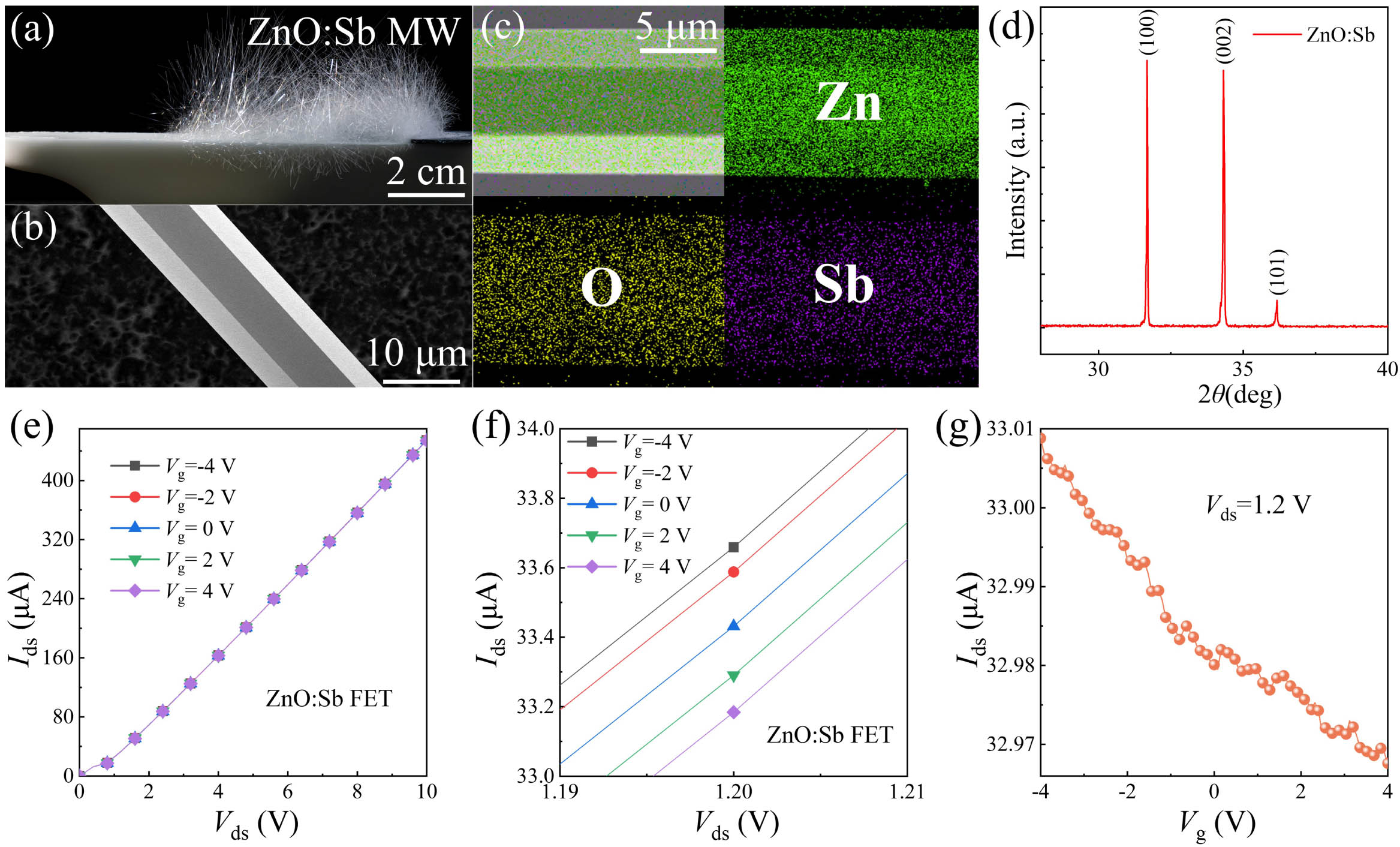
Fig. 1. Characterization of CVD-synthesized ZnO:Sb MWs. (a) Macroscopical photograph of ZnO:Sb MWs. (b) SEM picture of a single ZnO:Sb MW. (c) Elemental mapping images of Zn, O, and Sb species. (d) XRD patterns of ZnO:Sb samples. (e) Ids–Vds curves of the ZnO:Sb MW-based FET at different Vg. (f) Large view of Ids–Vds curves of the ZnO:Sb MW-based FET around Vds=1.2 V. (g) Transfer characteristic curve Ids–Vg of the ZnO:Sb MW-based FET at Vds=1.2 V.
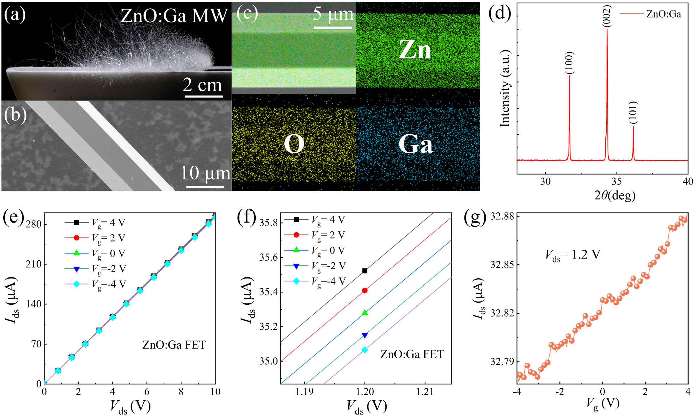
Fig. 2. Characterization of ZnO:Ga MWs. (a) Macroscopical photograph of CVD-synthesized ZnO:Ga MWs. (b) SEM image of a ZnO:Ga MW. (c) Elemental mapping images of Zn, O, and Ga species obtained from a ZnO:Ga MW. (d) XRD patterns of as-synthesized ZnO:Ga MWs. (e) Ids–Vds curves of the ZnO:Ga MW-based FET at different Vg. (f) Large view of Ids–Vds curves of the ZnO:Ga MW-based FET around Vds=1.2 V. (g) Ids–Vg curve of the ZnO:Ga MW FET at Vds=1.2 V.
Fig. 3. Characterization of as-constructed p-ZnO:Sb⊗n-ZnO:Ga MWs homojunction PD. (a) Schematic observation of the p-ZnO:Sb⊗n-ZnO:Ga MWs homostructure device. (b) Arrhenius dark current graph and R0A plot of the device at different temperature conditions. (c) Logarithmic I–V characteristic curves of the p-ZnO:Sb⊗n-ZnO:Ga MWs homostructure device in dark, and upon light illumination with the wavelengths ranging from 300 to 400 nm. (d) Variation of photo-to-dark current ratio Iph−Id at different wavelengths. (e) Wavelength-dependent R and D* when evaluated at −0.1 V bias. (f) Wavelength-dependent EQE and LDR when evaluated at −0.1 V bias.
Fig. 4. Photosensitivity characterization of the p-n homojunction PD when measured under 360 nm light irradiation via different optical intensities. (a) Logarithmic I–V characteristic curves of the PD in dark and under 360 nm light source illumination with the intensities varying from 0.1 to 5.0 mW/cm2. (b) Logarithmic plot of the photocurrent versus incident light intensity at −0.1 V bias. When evaluated at 360 nm light illumination: (c) R; (d) D*; (e) NEP; and (f) IPCE of PD as a function of light intensity at −0.1 V bias.
Fig. 5. Device stability and photosensitive mechanism of our constructed p-ZnO:Sb⊗n-ZnO:Ga MWs homojunction PD. (a) Bias-dependent I–t characteristic curves of the PD device under 360 nm light irradiation via 0.1 mW/cm2. (b) Changes of dark currents and photoresponse sensitivity versus the applied bias voltages when operated under 360 nm light illumination via 0.1 mW/cm2. (c) Normalized photocurrent intensity of the UV PD under irradiation of 360 nm light at −0.1 V bias. The inset is the stability of UV PD as a function of storage time. (d) Photoresponse speed to 360 nm pulse laser with a modulation frequency of 10 Hz at −0.1 V bias. (e) Energy band diagram of the p-n homojunction PD.
Fig. 6. Photoimaging application of our fabricated p-ZnO:Sb⊗n-ZnO:Ga an MWs homojunction UV PD. (a) Schematic design of the flexible integrated p-n homojunction array UV PD. (b) Optical photograph of a flexible MW homojunction array on PET substrate. (c) Microscopic image of a flexible MWs homojunction array. Scale bar: 200 μm. (d) Schematic diagram of the photoimaging measurement system. Inset in bottom right corner shows microscopic image of p-n homojunction array. Scale bar: 100 μm. (e) Imaging results of the optical patterns “MW” under 360 nm light source illumination. (f) Current waveform of the twelfth pixel acquired by the array unit. (g) Average photocurrents and signal-to-noise ratio under UV light illumination for the array unit.
Fig. 7. Schematic illustration of the single MW-based FET.
Fig. 8. Schematic illustration of the fabrication process for the p-ZnO:Sb⊗n-ZnO:Ga homojunction detectors.
Fig. 9. (a) Optical photograph of CVD-synthesized ZnO:Ga and ZnO:Sb MWs. (b) Microscopic image of MW under 180° bending angles.
Fig. 10. (a) Typical I-V characteristic curve of the device. Inset shows the microscopic image of the crossed MWs device. Scale bar: 100 μm. (b) Typical I-V characteristic curves of ZnO:Sb MW and ZnO:Ga MW.
Fig. 11. (a) Thermal imaging plot. (b) Dark current curves. (c) Dark current localized magnification curves of the device at different temperature conditions.
Fig. 12. Absorption versus wavelength (λ) plots of (a) ZnO:Ga MW and (b) ZnO:Sb MW. Inset is the Tauc curve from the corresponding absorption versus wavelength plots of ZnO:Ga MW and ZnO:Sb MW. (c) Photocurrent versus wavelength (λ) plots of the device at −0.1 V bias voltage. (d) Variation of photo-to-dark-current ratio Iph/Id of ZnO homojunction device at different UV light intensities. (e) Typical photoresponse of the device to 360 nm light source. (f) Typical pulse response of the device to 360 nm pulse laser.
Fig. 13. (a) Optical images of the ZnO homojunction array unit with various bending angles ranging from 0° to 90°. (b) I–t curves of the ZnO homojunction array unit under varied bending angles (the light illumination wavelength is 360 nm), and the corresponding light intensity is fixed at 0.2 mW/cm2. (c) Bending angle-dependent photocurrents. (d) I–t curves of the ZnO homojunction array unit with an increase of the bending cycles. (e) Variation of photocurrent with the increasing bending cycles.
Parameters | ZnO:Sb MW | ZnO:Ga MW |
---|
Diameter (μm) | 10 | 10 | Channel length (μm) | 150 | 150 | Carrier mobility () | 1.13 | 7.09 | Conductivity (S/cm) | 0.13 | 2.80 | Carrier density () | | |
|
Table 1. Electrical Transport Properties of As-Synthesized Individual ZnO:Sb and ZnO:Ga MWs
Photodetectors | Wavelength, Power | Bias (V) | | (A/W) | (Jones) | Refs. |
---|
Au-ZnO-Au | 365 nm, | 1 | 3.3 s/20 s | 0.01 | | [33] | ZnO (2D)/GaN (1D) | 352 nm, | 1 | — | 0.34 | | [34] | ZnO:Sb/ZnO nanowire | 365 nm, | 0 | 30 ms/30 ms | — | — | [35] | ZnO QD/ZnO film | 350 nm, | 10 | 1.56 s/1.82 s | 1.63 | | [41] | ZnO:Sb MW/ZnO MW | 386 nm, — | −5 | — | 0.2 | — | [43] | ZnO:Ag nanowire | 350 nm, | 0 | 1.09 s/5 s | — | — | [61] | ZnO nanofibers | 360 nm, | 0 | 3.90 s/4.71 s | 0.001 | — | [62] | Carbon-ZnO film-carbon | 365 nm, | 1 | 62.6 s/30.1 s | — | — | [63] | ZnO:Sb/ZnO nanorod | 365 nm, | −3 | 15.2 s/20.3 s | — | — | [64] | Au-ZnO nanofiber-Au | 350 nm, | 5 | 19.5 s/45.2 s | — | — | [65] | ZnO/NiO nanofiber | 350 nm, | 0 | 7.5 s/4.8 s | | — | [65] | | 360 nm, | −0.1 | 0.48 ms/79.41 ms | 2.3 | | This work |
|
Table 2. Comparison of Detection Performance Parameters of the ZnO-Based UV PDs