1College of Physics, MIIT Key Laboratory of Aerospace Information Materials and Physics, Key Laboratory for Intelligent Nano Materials and Devices, Nanjing University of Aeronautics and Astronautics, Nanjing 211106, China
【AIGC One Sentence Reading】:A ZnO microwire-based p-n homojunction photodiode offers high-performance UV detection with low power consumption, flexibility, and potential for integration into imaging systems.
【AIGC Short Abstract】:A ZnO-based homojunction photodiode, constructed from crossed p-type and n-type microwires, demonstrates excellent UV light detection with high responsivity, fast response, and superior photoelectron conversion efficiency. Its flexibility and stability make it suitable for wearable electronics and integrated photodetector arrays, enabling high-resolution single-pixel imaging, paving the way for low-power, flexible optoelectronic devices.
Note: This section is automatically generated by AI . The website and platform operators shall not be liable for any commercial or legal consequences arising from your use of AI generated content on this website. Please be aware of this.
Abstract
Low-power, flexible, and integrated photodetectors have attracted increasing attention due to their potential applications of photosensing, astronomy, communications, wearable electronics, etc. Herein, the samples of ZnO microwires having -type (Sb-doped ZnO, ZnO:Sb) and -type (Ga-doped ZnO, ZnO:Ga) conduction properties were synthesized individually. Sequentially, a homojunction vertical structure photodiode involving a single ZnO:Sb microwire crossed with a ZnO:Ga microwire, which can detect ultraviolet light signals, was constructed. When exposed under 360 nm light illumination at , the proposed photodiode reveals pronounced photodetection features, including a largest on/off ratio of , responsivity of 2.3 A/W, specific detectivity of Jones, noise equivalent power of , and superior photoelectron conversion efficiency of . The photodiode also exhibits a fast response/recovery time of 0.48 ms/9.41 ms. Further, we propose a facile and scalable construction scheme to integrate a microwires homojunction component into a flexible, array-type detector, which manifests significant flexibility and electrical stability with insignificant degradation. Moreover, the as-constructed array unit can be integrated into a practical photoimaging system, which demonstrates remarkable high-resolution single-pixel imaging capability. The results represented in this work may supply a workable approach for developing low-dimensional ZnO-based homojunction optoelectronic devices with low-consumption, flexible, and integrated characteristics.
1. INTRODUCTION
In recent years, the flexible and integrated ultraviolet photodetector (UV PD) has become a crucial active component for photosensing, optical communications, wearable devices, foldable displays, etc. [1–5]. To satisfy the ever-increasing demands of realistic applications, the construction of flexible and integrated photodiodes should necessarily mandate advantages such as low energy consumption, low dark current, fast response time, high mechanical stability, etc. [6–8]. In previous studies, low-dimensional organic and inorganic materials, such 0D quantum dots, 1D micro-/nanostructures, and 2D layered materials have been extensively used to fabricate flexible and integrated devices [9–15]. However, the PDs based on 0D and 2D materials have several drawbacks owing to material intrinsic problems and complex fabrication techniques [16,17]. For example, the solution-synthesized 0D materials are prone to problems such as instability, low photogenerated charge carrier density, poor charge transport, and so on, which seriously hinder further applications of quantum dot-based flexible photovoltaic devices [18–21]. Additionally, although significant progress has been achieved in developing flexible optoelectronic devices based on the 2D layered materials. The presence of poorer light absorption, large-scale, complex preparation process, difficult transfer, poor ductility, etc., also makes them unable to carry out large-area practical applications [22–24]. In contrast, 1D micro-/nanostructure materials have been widely applied in flexible detectors because of their superior mechanical stability, high carrier mobility, high surface-to-volume ratio, and simple synthesis [17,25]. In particular, assembling these 1D micro-/nanostructures into highly ordered arrays as ideal building blocks can realize the low-power, flexibility, and integration practical applications for novel optoelectronic devices [26–28].
ZnO, an important third-generation semiconductor, has been widely considered as potential material for the construction of UV PDs owing to the low cost, abundance of raw materials, nontoxicity, large bandgap of 3.37 eV, and high exciton binding energy of 60 meV [29–31]. Low-dimensional ZnO, including nanofibers, microwires (MWs), nanowires, and so on, has attracted extensive scientific interest in flexible detectors owing to their large length/diameter ratio, miniaturization, and flexibility. Generally, there are three types of detectors: metal-semiconductor-metal (MSM); Schottky; and junction [1,32–35]. The limitations of a typical MSM structure detector such as complex metal electrode contacts, large operating voltage, and low photoresponse would inevitably restrict the development toward low-power consumption, flexibility, and integration [1,32,36,37]. Compared with photovoltaic junction detectors, the traditional Schottky devices usually suffer from numerous bottlenecks, such as serious absorption of metal electrodes, relatively thinner depletion layer, and photocarriers transporting barriers. These shortcomings severely hinder the further application of Schottky-based PDs [38–40]. The realization of junction photodiodes has received widespread attention owing to its excellent photodetection properties. Because of the lattice mismatch, heterojunction interface discontinuity of energy levels, etc., heterojunctions usually have numerous defects, such as trapping states, large leakage current, surface defects, and high strains, thus bringing about economic difficulties in constructing high-performance heterojunction photodiodes [41–44]. Currently, the achievement of ZnO-based homojunction photodiodes has been blocked by the presence of high-quality -type ZnO. Developing ZnO homojunction UV detectors that meet the requirements of low power consumption, high-performance, flexibility, integrability, and practical applicability remains a long-term and arduous task [4,45,46].
In this work, the sample of Ga-doped ZnO (ZnO:Ga) MWs showing -type conductivity was synthesized individually, while the product of -type conductivity ZnO MWs, which were doped with Sb-dopant (ZnO:Sb), was also obtained. The conducting properties were subsequently further verified using single MW-based field-effect transistors (FETs). A vertically structured homojunction containing ZnO:Sb MW crossed with ZnO:Ga MW was constructed, showing excellent UV photodetection capability. When operated under 360 nm light irradiation at , the largest responsivity, detectivity, on/off ratio, noise equivalent power, and photoelectron conversion efficiency can reach , , , , and 7.8%, respectively. The device also exhibited a fast rise/decay speed (). Further, the PD could be integrated into large-scale flexible optoelectronic arrays, which shows small degradation in the photocurrent after 400 bending cycles. Interestingly, the array unit as a pixel sensor exhibits its huge potential for UV imaging. This work offers a novel approach to design and fabricate high-performance, low-power, flexible, and integrable optoelectronic devices.
Sign up for Photonics Research TOC. Get the latest issue of Photonics Research delivered right to you!Sign up now
2. EXPERIMENTAL SECTION
A. Preparation of ZnO:Ga MW and ZnO:Sb MW
In the present study, the sample of MWs was synthesized using a chemical vapor deposition (CVD) method [47,48]. The rational preparation of samples with tunable -type conductivity is available using as the doping source. In the synthesis process of individual ZnO:Ga MWs, the precursor mixture containing ZnO, , and graphite (C) powder with a weight ratio of 9:1:10 served as source materials. Using the CVD method, individual ZnO:Ga MWs were successfully obtained. Compared with the preparation of -type ZnO:Ga MW, the Sb element is commonly used to substitute Zn to induce -type conductivity. The experimental scheme has been illustrated in our previous literature [29,49]. In the synthesis process of individual ZnO:Sb MW, a powder mixture of ZnO, , and C high purity powder (99.99%) in a weight ratio of approximately 9:1:10 was used as the source.
B. Fabrication of MW-Based FET and Homojunction Device
To investigate the electronic transport properties of CVD-prepared samples, an MW-based FET was fabricated by combining substrate [50]. First, a single MW was mechanically transferred to the cleaned wafer. Second, the Ti/Au serving as source and drain electrodes were welded at both the ends of the wire, while the Si substrate was used as the global back gate electrode for the FETs. The corresponding schematic illustration of the single MW-based FET is shown in Fig. 7 in Appendix A.
A representative cross-stacked homojunction device is constructed, which consists of a single -type ZnO:Sb MW crossed with another -type ZnO:Ga MW in a cross-shape layout, with each MW having a matching electrode forming an ohmic contact with it, respectively. The detailed fabrication process is summarized as follows: (i) deposition of thick and μ wide Au channel electrode on sapphire using an electron-beam evaporation method (Å); (ii) 5 μm thick MgO blocking layers were deposited on both sides of the Au channel electrode (Å); (iii) a ZnO:Sb MW was placed on the Au channel electrode; (iv) the other ZnO:Ga MW was then transferred to cross over the ZnO:Sb MW; (v) deposition of μ blocking layer on the indium tin oxide (ITO), leaving μ of the ITO channel was utilized as the top electrode; and (vi) using ITO to apply pressure to the crossed areas of the MW, which in turn makes good physical contact between the crossed samples. The corresponding schematic diagram of the detailed construction process of the device is shown in Fig. 8 in Appendix B.
C. Characterization
The morphology and structure of CVD-synthesized ZnO:Ga and ZnO:Sb MWs were characterized using a scanning electron microscope (SEM) (TESCAN LAYRA3 GM). The chemical compositions of samples were detected using an energy-dispersive spectrometer (EDS), which was attached to the SEM. The crystal structure of the samples was characterized using X-ray diffraction (XRD) (Malvern Panalytical, Empyrean). The optical photograph of samples was obtained by the microscope (Olympus, BX53M). Photoelectrical properties of the constructed devices were conducted using a semiconductor analyzer (Keysight, B1500A), a light source (EQ99X), and a monochromator (Zolix, Omni-). The temperature of the device was tested using a handheld thermal imaging camera (FOTRIC 321Q). The response speed of PD devices was evaluated by connecting the detector with a resistor. A 365 nm Nd:YAG pulsed laser (Ekspla, NT342) and a digital oscilloscope (Tektronix, DPO 2012B) were used as the light source and data collection, respectively.
3. RESULTS AND DISCUSSION
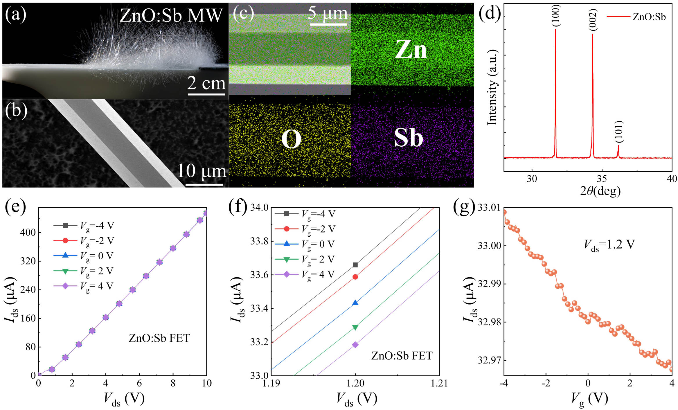
Figure 1(a) presents the optical photograph of the CVD-prepared ZnO:Sb MW, and a single ZnO:Sb MW sample was successfully picked out by using a facile mechanical transfer method. The corresponding surface morphology of a single ZnO:Sb MW in Fig. 1(b) was obtained by the SEM, where the image displays that the sample exhibits a regular hexagonal prismatic structure, smooth and straight sidewall facets, and sharp edges. The chemical composition of the ZnO:Sb wire was characterized via EDS mapping. As shown in Fig. 1(c), the homogeneous distribution of the Sb element was witnessed, indicating that a high degree of homogeneity of Sb doping was successfully achieved in the synthesis of ZnO:Sb MWs. The phases and crystal structure of CVD-synthesized ZnO:Sb wires were further tested via XRD scanning at a two-diffraction angle ranging from 26° to 40°. The XRD result in Fig. 1(d) shows diffraction peaks positioning at 32.65°, 34.32°, and 36.15°, which are assigned to the (100), (002), and (101) planes, respectively. Thus, the CVD-grown ZnO:Sb MWs are belonging to crystalline hexagonal phase of ZnO (JCPDS No. 36–1451). Further, the diffraction peaks of the samples are relatively sharp without any additional phases, indicating that the synthesized samples have excellent crystalline quality. Further, the microscopic image of the sample [Figs. 9(a) and 9(b) in Appendix C] shows that a high aspect ratio ZnO:Sb MW has uniform morphology and good mechanical flexibility, which benefits its applications in flexible optoelectronic devices.
Figure 1.Characterization of CVD-synthesized ZnO:Sb MWs. (a) Macroscopical photograph of ZnO:Sb MWs. (b) SEM picture of a single ZnO:Sb MW. (c) Elemental mapping images of Zn, O, and Sb species. (d) XRD patterns of ZnO:Sb samples. (e) curves of the ZnO:Sb MW-based FET at different . (f) Large view of curves of the ZnO:Sb MW-based FET around . (g) Transfer characteristic curve of the ZnO:Sb MW-based FET at .
Figure 2.Characterization of ZnO:Ga MWs. (a) Macroscopical photograph of CVD-synthesized ZnO:Ga MWs. (b) SEM image of a ZnO:Ga MW. (c) Elemental mapping images of Zn, O, and Ga species obtained from a ZnO:Ga MW. (d) XRD patterns of as-synthesized ZnO:Ga MWs. (e) curves of the ZnO:Ga MW-based FET at different . (f) Large view of curves of the ZnO:Ga MW-based FET around . (g) curve of the ZnO:Ga MW FET at .
Figure 3.Characterization of as-constructed MWs homojunction PD. (a) Schematic observation of the MWs homostructure device. (b) Arrhenius dark current graph and plot of the device at different temperature conditions. (c) Logarithmic characteristic curves of the MWs homostructure device in dark, and upon light illumination with the wavelengths ranging from 300 to 400 nm. (d) Variation of photo-to-dark current ratio at different wavelengths. (e) Wavelength-dependent and when evaluated at bias. (f) Wavelength-dependent EQE and LDR when evaluated at bias.
Figure 4.Photosensitivity characterization of the homojunction PD when measured under 360 nm light irradiation via different optical intensities. (a) Logarithmic characteristic curves of the PD in dark and under 360 nm light source illumination with the intensities varying from 0.1 to . (b) Logarithmic plot of the photocurrent versus incident light intensity at bias. When evaluated at 360 nm light illumination: (c) ; (d) ; (e) NEP; and (f) IPCE of PD as a function of light intensity at bias.
Figure 5.Device stability and photosensitive mechanism of our constructed MWs homojunction PD. (a) Bias-dependent characteristic curves of the PD device under 360 nm light irradiation via . (b) Changes of dark currents and photoresponse sensitivity versus the applied bias voltages when operated under 360 nm light illumination via . (c) Normalized photocurrent intensity of the UV PD under irradiation of 360 nm light at bias. The inset is the stability of UV PD as a function of storage time. (d) Photoresponse speed to 360 nm pulse laser with a modulation frequency of 10 Hz at bias. (e) Energy band diagram of the homojunction PD.
Figure 6.Photoimaging application of our fabricated an MWs homojunction UV PD. (a) Schematic design of the flexible integrated homojunction array UV PD. (b) Optical photograph of a flexible MW homojunction array on PET substrate. (c) Microscopic image of a flexible MWs homojunction array. Scale bar: 200 μm. (d) Schematic diagram of the photoimaging measurement system. Inset in bottom right corner shows microscopic image of homojunction array. Scale bar: 100 μm. (e) Imaging results of the optical patterns “MW” under 360 nm light source illumination. (f) Current waveform of the twelfth pixel acquired by the array unit. (g) Average photocurrents and signal-to-noise ratio under UV light illumination for the array unit.
Figure 10.(a) Typical I-V characteristic curve of the device. Inset shows the microscopic image of the crossed MWs device. Scale bar: 100 μm. (b) Typical I-V characteristic curves of ZnO:Sb MW and ZnO:Ga MW.
Figure 11.(a) Thermal imaging plot. (b) Dark current curves. (c) Dark current localized magnification curves of the device at different temperature conditions.
Figure 12.Absorption versus wavelength () plots of (a) ZnO:Ga MW and (b) ZnO:Sb MW. Inset is the Tauc curve from the corresponding absorption versus wavelength plots of ZnO:Ga MW and ZnO:Sb MW. (c) Photocurrent versus wavelength () plots of the device at bias voltage. (d) Variation of photo-to-dark-current ratio of ZnO homojunction device at different UV light intensities. (e) Typical photoresponse of the device to 360 nm light source. (f) Typical pulse response of the device to 360 nm pulse laser.
Figure 13.(a) Optical images of the ZnO homojunction array unit with various bending angles ranging from 0° to 90°. (b) curves of the ZnO homojunction array unit under varied bending angles (the light illumination wavelength is 360 nm), and the corresponding light intensity is fixed at . (c) Bending angle-dependent photocurrents. (d) curves of the ZnO homojunction array unit with an increase of the bending cycles. (e) Variation of photocurrent with the increasing bending cycles.
The electrical transport properties of individual Sb-doped MW were researched using FETs [36]. Figure 1(e) shows a set of typical current and source-drain voltage () data under different gate voltage ( ranges from to 4 V). The linear feature of the plotted curves confirms that the metal electrodes make good ohmic contacts with the single wire. This is further confirmed by the local magnification curve of the [Fig. 1(f)]. The versus curve for the FET recorded at is shown in Fig. 1(g). Electrical analysis shows that the conductance of the FET increases (decreases) with increasingly negative (positive) . In consequence, a significant modulation of the typical -type electrical transport properties of single MW was successfully realized via a simple Sb-doping.
Figure 2(a) shows a representative photograph of CVD-prepared ZnO:Ga MWs, which exhibits outwardly dispersing needle-like growth, indicating an excellent aspect ratio of the synthesized samples. According to the SEM result of a single ZnO:Ga MW in Fig. 2(b), the morphology of wire is a hexagonal prism with a diameter of μ. Moreover, the ZnO:Ga MW possesses a uniform morphology throughout its entire length with smooth and flat surfaces. The Ga element distribution is measured in Fig. 2(c) via EDS mapping analysis. It is apparent that the Ga component is uniformly distributed in the ZnO:Ga MWs, indicating that Ga elements can be well incorporated into the ZnO lattice. Figure 2(d) shows the XRD pattern of the samples, in which all the diffraction peaks can be well indexed to the hexagonal wurtzite phase of ZnO. Further, the value of full-width at half-maximum for the (002) plane is 0.071°, manifesting excellent crystal quality of CVD-synthesized samples.
Similarly, the electrical properties of a ZnO:Ga MW can be clarified on the basis of single-wire backgated FETs. Typical versus curves under varied are shown in Fig. 2(e). The enlarged result of the output characteristic curve clearly exhibits a typical linear feature of the device [see Fig. 2(f)]. The transport characteristic curve for the device recorded at is shown in Fig. 2(g). The result shows that the device exhibits a noticeable gating effect, and increases with increasing , which is a typical behavior of the -type electronic transport properties of our synthesized ZnO:Ga wires [51].
Further, the carrier mobility (), conductivity (), and carrier density () in CVD-synthesized ZnO:Sb and ZnO:Ga MWs were estimated by fitting the curve, respectively. The carrier mobility can be calculated due to , where and are the capacitance and the channel length of single wire, respectively [37]. The capacitance is given by , in which , , , and are the vacuum dielectric constant, relative dielectric constant of , thickness of the , and diameter of the wire, respectively [36]. The conductivity can be calculated according to , where , , , and are the resistance, resistivity, conductivity, and cross-sectional area of the MW, respectively. The carrier density can be determined by , where is the elementary charge [30]. Therefore, the carrier mobility, conductivity, and carrier density of ZnO:Sb MWs and ZnO:Ga MWs are as shown in Table 1. The result shows that the corresponding electrical parameters of the ZnO:Ga MW are evidently better than those of ZnO:Sb MW, suggesting that Sb doping can achieve the change of conduction behavior from - to -type [47].
Electrical Transport Properties of As-Synthesized Individual ZnO:Sb and ZnO:Ga MWs
Parameters
ZnO:Sb MW
ZnO:Ga MW
Diameter (μm)
10
10
Channel length (μm)
150
150
Carrier mobility ()
1.13
7.09
Conductivity (S/cm)
0.13
2.80
Carrier density ()
Figure 3(a) shows that a representative cross-shape device was constructed by using a vertical structure, which consists of two MWs in a cross-shape layout, with the ITO and Au films acting as contact electrodes for the ZnO:Ga and ZnO:Sb MWs, respectively. An curve in the dark of the constructed device is displayed in Fig. 10(a) in Appendix D. The curve shows that a -type ZnO:Sb MW crossed with -type ZnO:Ga MW () exhibits clear current rectification characteristic with a turn-on voltage of , after which the forward current increases rapidly. The inset in Fig. 10(a) in Appendix D shows an optical photograph of the constructed device. Figure 10(b) (in Appendix D) exhibits that the measurements made on the individual ZnO:Sb and ZnO:Ga MWs show a linear response characteristic of ohmic contacting features. It suggests that the rectification characteristic is mainly attributed to the fabricated crossed-shape MWs device, illustrating that a high-quality homojunction is formed in the physical contact region toward the interface. To obtain clearer insight into the temperature dependence of the dark current behavior [dark current versus voltage measured at different temperatures as shown in Figs. 11(a)–11(c) in Appendix E], we represent the dark current and the resistance-area product () using an Arrhenius plot, as shown in Fig. 3(b). It is found that varying the temperature from 260 to 330 K, the dark current exhibits a considerably linear increase. This phenomenon may be derived from the fact that the low temperature would lead to a slower transport efficiency of the interfacial diffusion current, which in turn weakens the dark current. Also, the product at 330 K is evaluated to about . It also increases to as the temperature reduces to 260 K. The higher value of results from the tiny junction region interface. In this case, the change through diminishing the surface leakage current would lead to the reduced dark current of as-constructed devices [52].
The photoelectrical properties of the MW homojunction device were systematically tested under light illumination with different wavelengths. As depicted in Fig. 3(c), the logarithmic characteristic curves under several selected wavelengths (300, 320, 340, 360, 380, and 400 nm) were measured. It can be found that the device has a pronounced photoresponse behavior and shows the largest photocurrent at the wavelength of 360 nm. Figure 3(d) shows that the photo–dark current ratio of the homojunction device can reach as high as at bias. Additionally, room temperature absorption versus wavelength () plots of ZnO:Ga and ZnO:Sb MWs and the logarithmic characteristic curves of the device in the range of 200–600 nm are shown in Figs. 12(a) and (b) in Appendix F. The absorption edges of the samples appear at 380 nm without any shift for ZnO:Ga and ZnO:Sb samples, indicating that the modulation effect of doping via introducing electron donor (Ga) or acceptor (Sb) elements into the ZnO host crystal on absorption characteristics could be negligible. The optical bandgaps of CVD-grown ZnO:Ga MW and ZnO:Sb MW were calculated to be 3.19 and 3.21 eV, respectively. Compared with bulk ZnO, the deviations could be derived from the self-absorption of CVD-synthesized monocrystalline wirelike structures. Figure 12(c) in Appendix F shows a wavelength-dependent photoresponse at the ultraviolet wavelengths. Owing to the excellent light absorption properties of the samples, the constructed devices exhibit a pronounced photoresponse at the UV wavelengths, with the strongest response occurring at 360 nm.
To quantitatively evaluate the photodetection properties of homojunction PD, several critical performance parameters, including photocurrent responsivity (), specific detectivity (), external quantum efficiency (EQE), and linear dynamic range (LDR), were considered. These parameters are described below [40,53,54]: where is the effective irradiated area () of device; is the incident power intensity (); and are the photocurrent and dark current of the homojunction PD, respectively; is the electron charge constant (); is the Planck constant (); is the speed of light (), and is the wavelength of incident light.
The effect of light irradiation at different wavelengths on the performance of the homojunction PD was researched. The and at were calculated using Eqs. (1) and (2), respectively. Figure 3(e) demonstrates that the largest can reach 2.32 A/W at a wavelength of 360 nm; thereby, the UV/visible rejection ratio was achieved, which indicates that the homojunction PD has outstanding detection ability for UV lights, whereas the higher spectral response can be attributed to the absorption characteristics of CVD-synthesized samples. In addition, we found that the reaches the maximum value of at 360 nm and maintains the same order of in a broad UV wavelength range, which is superior to most previously reported ZnO-based homojunction detectors [41]. The EQE and LDR at different wavelengths obtained from Eqs. (3) and (4) are shown in Fig. 3(f). The EQE data shows that the PD exhibits high photoelectric conversion efficiencies in the range of 300–400 nm, and the highest EQE value is achieved at the wavelength of 360 nm. The calculated LDR values are averagely evaluated to at UV wavelengths of 300–400 nm, which is comparable with those of commercial photodetectors [55]. In particular, the largest LDR can raise up to 80 dB at the wavelength of 360 nm, which indicates that the fabricated detector has excellent signal-to-noise ratio.
To evaluate the photodetecting performance of the homojunction PD under 360 nm light irradiation at , we performed characteristics tests of the PD under different light intensities ranging from 0 to , as shown in Fig. 4(a). It clearly illustrates that the photocurrent exhibits an observable enhancement with increasing light intensities. The photo–dark current ratio of the PD increases from () to at bias [Fig. 12(d) in Appendix F]. The robust increase of the photo–dark current ratio can be attributed to the fact that the higher intensity of the incoming lights induces more photocarriers, in turn, enhancing the photocurrent response. Figure 4(b) presents the changes of the obtained photocurrents versus the light illumination intensity of the PD at bias. The change can be well fitted by the power law [40] where is a constant at a specific wavelength, and is a power-law factor. The value is estimated to be 0.90 (ideal value is 1), suggesting that interfacial recombination loss in the homojunction could be neglected upon UV light irradiation. We also noted the linear character of the photocurrent via light illumination intensity, which is different from low-dimensional ZnO heterojunction photodiodes. Such an experimental phenomenon is mainly caused by the existence of fewer interface defects acting as the charge recombination centers in homojunction. Thus, the trapping centers are rapidly saturated upon UV light illumination, which effectively reduces recombination loss resulting from the growing concentration of photogenerated carriers in homojunction interface [39].
The illumination density-dependent photoresponse performances of the homojunction PD were studied at the wavelength of 360 nm. Figures 4(c) and 4(d) demonstrate that the and show a decreasing trend when increasing the light intensity of the incident light. That is, the largest () and () can be achieved under weak light density of UV irradiation, indicating the outstanding photosensitivities of the PD to weak UV light signals. The reduced visibility of the obtained photosensitive properties with increasing light intensity could be probably attributed to the surface and interfacial defects of ZnO:Sb and ZnO:Ga MWs as well as the constructed devices. In that case, a small part of the photocarriers may be recombined before being collected by electrodes, decreasing the average lifetime with the increasing carrier recombination rate [56].
The NEP and IPCE of the homojunction PD were analyzed according to the following equations [56,57]: where and are the electron charge constant and dark current, respectively. and are the measured photocurrent density and light intensity at a fixed wavelength (). The variation of NEP as a function of different light intensities is plotted in Fig. 4(e) at bias. As the UV light intensity increases, the NEP increases gradually, indicating that the PD shows lower NEP () at the weak light signals. This phenomenon can be attributed to the tiny contact area between the ZnO:Sb and ZnO:Ga MWs, which effectively reduces the background noise caused by the much lower interfacial defect states. Figure 4(f) depicts the changes of IPCE versus optical densities of the incoming light, which were calculated by using Eq. (7). The observed negative relationship could be speculated to the fact that the internal gain effect of the PD diminishes with increasing UV light irradiance density [32,58]. Therefore, the PD gives a maximum IPCE of 7.8% upon the 360 nm light irradiation.
To access the stabilities of the homojunction PD, the curves of the device at different reverse voltages are displayed in Fig. 5(a). The current has a strong dependence on the reverse bias. Further, the fabricated PD shows a superior time-dependent photoresponse even at low bias along with excellent reproducibility and stability, which is considered to be a critical factor for practical application in low-power devices. The dark current and photoresponse sensitivity as a function of different reverse bias are as plotted in Fig. 5(b). The results demonstrate that the photoresponse sensitivity decreases with increasing dark currents under reverse bias condition, where the sharply increased dark current may be attributed to the avalanche multiplication of carriers in the depletion layer caused by the larger reverse bias [58]. The environmental stability of the unencapsulated homojunction PD was tested. In the measurement, the photocurrent intensity was recorded under continuous irradiation of 360 nm light () at room temperature (25°C) and humidity. As shown in Fig. 5(c), the device has only fluctuation of photocurrent intensity after prolonged UV irradiation. Meanwhile, the inset of Fig. 5(c) shows that the environmental stability of the PD was discussed as a function of storage time (15, 30, and 60 days later). Although the photocurrent intensity fluctuated after 60 days of storage, the device also maintained over 90% of the pristine photocurrent, indicating that the device can ensure long-term stable operation even in an unencapsulated state.
The response speed of the homojunction PD was examined by measuring its rise (10%–90%) and decay (90%–10%) upon switching the UV irradiation on and off. As shown in Fig. 12(e) in Appendix F, the and are estimated to be 0.073 and 0.392 s, respectively. The much lower response speed could result from the test limits of the semiconductor parametric analysis instrument. To actually approach the response speed, the transient photoresponse of our as-fabricated homojunction PD was conducted under a 360 nm pulse laser illumination at . As shown in Fig. 12(f) in Appendix F, the captured pulse signals with steady, rapid, and repeatable photoresponse are clearly obtained. Figure 5(d) exhibits a single pulse of the time-resolved photoresponse; thereby the and can be derived to about 0.48 and 79.41 ms, respectively. The fast response speed of the PD was superior to most of previously reported ZnO-based homojunction detectors. It is mainly attributed to the cooperative effect of composite (external and built-in) electric fields at the junction interface and the formation of high-quality homojunction with fewer trap states; thus, it is conducive to the quick separation and transport of photoinduced carriers [35,59,60].
The photosensitive mechanism and photocarrier transport paths of our as-fabricated homojunction device can be further understood by the energy band diagram, as shown in Fig. 5(e). Shown in the photograph (left), , , and are the conduction band, valence band, and Fermi energy level of CVD-synthesized ZnO:Sb and ZnO:Ga samples, respectively. and are their bandgap energies and electron affinity, respectively. It has been reported that the bandgap energy and electron affinity values of ZnO are 3.37 and 4.35 eV, respectively [Fig. 5(e)-I] [59]. As both MWs are in contact with each other, the difference in Fermi levels would lead to the majority carriers interdiffusion between the ZnO:Ga MW (for the electrons) and ZnO:Sb MW (for the holes). When the device is in an equilibrium state, built-in potential is established [see Fig. 5(e)-II]. The depletion layer thickness () created in ZnO:Sb and ZnO:Ga samples at 0 V bias can be estimated using the formula [54] where and are relative dielectric constant of ZnO:Sb and ZnO:Ga MW, respectively. (, ZnO:Ga) is carrier densities of ZnO:Sb and ZnO:Ga MW, respectively. is the built-in field intensity of the PD, is the elementary charge, and is vacuum dielectric constant. The of ZnO:Sb and ZnO:Ga MW are estimated to be and , respectively. The depletion layer thickness of the homojunction PD is about 10.79 nm at 0 V bias. However, once the PD is operated upon UV light illumination at bias, photoinduced generation of electron-hole pairs will be formed in the depletion layer and then could be separated by combining the external electric field and the built-in electric field [Fig. 5(e)-III]. In this case, the external electric-field associated with the preformed built-in potential is more favorable for photocarriers transport. As summarized in Table 2, the homojunction PD in this research exhibits much better photosensitive performance than other previously reported ZnO-based UV PDs.
Comparison of Detection Performance Parameters of the ZnO-Based UV PDs
Photodetectors
Wavelength, Power
Bias (V)
(A/W)
(Jones)
Refs.
Au-ZnO-Au
365 nm,
1
3.3 s/20 s
0.01
[33]
ZnO (2D)/GaN (1D)
352 nm,
1
—
0.34
[34]
ZnO:Sb/ZnO nanowire
365 nm,
0
30 ms/30 ms
—
—
[35]
ZnO QD/ZnO film
350 nm,
10
1.56 s/1.82 s
1.63
[41]
ZnO:Sb MW/ZnO MW
386 nm, —
−5
—
0.2
—
[43]
ZnO:Ag nanowire
350 nm,
0
1.09 s/5 s
—
—
[61]
ZnO nanofibers
360 nm,
0
3.90 s/4.71 s
0.001
—
[62]
Carbon-ZnO film-carbon
365 nm,
1
62.6 s/30.1 s
—
—
[63]
ZnO:Sb/ZnO nanorod
365 nm,
−3
15.2 s/20.3 s
—
—
[64]
Au-ZnO nanofiber-Au
350 nm,
5
19.5 s/45.2 s
—
—
[65]
ZnO/NiO nanofiber
350 nm,
0
7.5 s/4.8 s
—
[65]
360 nm,
−0.1
0.48 ms/79.41 ms
2.3
This work
The potential application of the homojunction PD in flexible integrated optoelectronic devices was further researched. The schematic architecture of the flexible integrated homojunction array based on a single unit of our preprepared homojunction device is illustrated in Fig. 6(a). We fabricated an array unit of the PD in a μμ area. First, Au electrodes were deposited on the flexible PET substrate, then ZnO:Sb MW and ZnO:Ga MW were welded on the Au electrodes by indium, and finally the device was simply covered with polymethyl methacrylate (PMMA). Figure 6(b) represents the optical photograph of a flexible integrated PD array unit on PET substrate; the corresponding microscopic photograph is shown in Fig. 6(c). The microscopic photograph of the device shows that all the ZnO:Ga MWs form good contacts with ZnO:Sb MWs. Meanwhile, to study the stability of the PD array unit under harsh conditions, the photocurrents of the device were measured after it was subjected to various bending angles and bending cycles, as shown in Figs. 13(a)–13(e) in Appendix G. It demonstrates that the photocurrent of the fabricated PD array unit remained fairly stable up to 30° bending angles and 50 bending cycles, keeping more than 80% of its initial photocurrent value even after 90° bending angles and 400 bending cycles. This reveals the potential of the PD array unit for versatile applications in flexible and integrated optoelectronic devices.
Finally, the proposed homojunction PD has great potential for single pixel photoimaging, which is important functional components for information communication, image sensors, and flexible optoelectronic devices. However, high-performance flexible homojunction PD with high resolution and stable photoresponse still need to be developed. Figure 6(d) shows the schematic diagram of the MW imaging measurement platform, which consists of the PD array unit, light source, lens assembly, 2D translation stage, and so on. Figure 6(e) shows an efficiently detected image of the “MW” letters collected by the array unit under 360 nm light source illumination at . Obviously, the device exhibits high contrast and resolution with sharp edges. As shown in Fig. 6(f), the current waveform of the twelfth pixel [position of the red line in Fig. 6(e)] is acquired by the array unit, which suggests that the device has the ability to track rapidly varied light signals. The average photocurrent and SNR of the device were obtained under different scanned pixels, as demonstrated in Fig. 6(g). The imaging results clearly indicate the excellent imaging capability and superior signal current uniformity of the device as a single sensing pixel. It is notable that the SNR of the array unit is all more than 50 dB, and the high SNR values reveal the outstanding low-light detection capability of the device, suggesting that the homojunction array unit can efficiently convert UV light into photocurrents. Therefore, the homojunction PD as a UV signal receiving terminal can provide new ideas for the design and fabrication of miniaturized, low-power, and high-performance flexible integrated UV imaging sensor devices.
4. CONCLUSIONS
In summary, we have successfully constructed a high-performance flexible UV PD based on a MWs homojunction. The device can work at a relatively low operation voltage, suggesting its low-power consumption detection. The PD exhibits an impressive overall photosensitive property, including a largest responsivity of 2.3 A/W, a large specific detectivity of , a superior NEP of , an excellent IPCE of 7.8%, and fast response speed (0.48 ms/79.41 ms) under 360 nm light illumination at . These comparable figure-of-merit parameters show that the homojunction device demonstrates its remarkable potential for UV imaging, optical communication, and biological detection. As a unit of MWs homojunction was integrated into a flexible array, the device exhibits less than 20% degradation in photodetection performance after 90° angles and 400 times bending-releasing test, indicating its good mechanical flexibility and stability. Moreover, the fabricated PD array unit was also integrated into a string array pixel, giving rise to high-resolution imaging capabilities. Given their UV photodetection properties, excellent mechanical flexibility and stability, and photosensitive imaging, we believe that the as-constructed MWs homojunction PD will boost the progress toward next-generation wearable technologies and integrated UV imaging sensor.
APPENDIX A: SCHEMATIC VIEW OF FIELD-EFFECT TRANSISTORS
Figure 7 shows the schematic diagram of the FET device structure, including a single microwire, source and drain electrodes, and the global back gate electrode.
APPENDIX B: CONSTRUCTION PROCESS OF DEVICE
Figure 8 presents the detail information on the process of photodetection device fabrication.
APPENDIX C: PHOTOGRAPH OF CVD-PREPARED MWS
Figure 9 illustrates optical photographs of CVD-prepared ZnO:Ga and ZnO:Sb MWs, the enlarged wire samples, and a microscope photograph of a single MW bent through 180°.
APPENDIX D: ELECTRICAL CHARACTERISTICS OF DEVICE AND MWS
Figure 10 demonstrates the rectification characteristics of the constructed homojunction device, the microscopic photograph of the corresponding device, and the I-V characteristic curves of the ZnO:Sb and ZnO:Ga MWs, respectively.
APPENDIX E: THERMAL IMAGE AND DARK CURRENT OF DEVICE
Figure 11 displays the thermal images of the constructed homojunction devices at different conduction temperatures (from 260 to 330 K), and the dark current versus voltage plots of the devices.
APPENDIX F: ABSORPTION OF MWS AND PERFORMANCE OF DEVICE
Figure 12 exhibits the absorption versus wavelength () for ZnO:Ga and ZnO:Sb MW samples, the light-to-dark current ratio, and the response speed of the p-ZnO:Sb⊗n-ZnO:Ga MW homojunction device.
APPENDIX G: FLEXIBILITY OF DEVICE
Figure 13 shows the optical images of the constructed homojunction array unit at different bending angles (0° to 90°), the I–t curves for different bending angles and bending times.
 AI Video Guide
  AI Picture Guide
 AI One Sentence