- Photonics Research
- Vol. 7, Issue 7, 711 (2019)
References
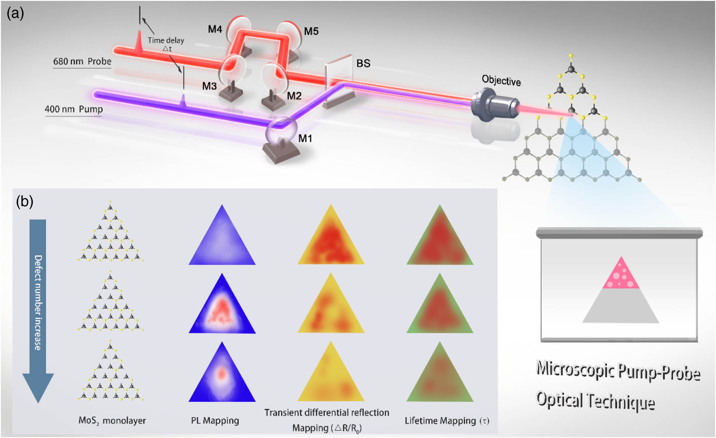

Ying Yu, Xiankun Zhang, Zhangkai Zhou, Zheng Zhang, Yanjun Bao, Haofei Xu, Limin Lin, Yue Zhang, Xuehua Wang. Microscopic pump-probe optical technique to characterize the defect of monolayer transition metal dichalcogenides[J]. Photonics Research, 2019, 7(7): 711
Download Citation

Set citation alerts for the article
Please enter your email address
© Copyright 2018-2021 | Chinese Laser Press. All Rights Reserved 沪ICP备15018463号-20