Abstract
Monolayer transition metal dichalcogenides (TMDs) are ideal materials for atomically thin, flexible optoelectronic and catalytic devices. However, their optoelectrical performance such as quantum yield and carrier mobility often shows below theoretical expectations due to the existence of defects. For monolayer TMD-based devices, finding a low-cost, time-efficient, and nondestructive technique to visualize the change of defect distribution in the space domain and the defect-induced change of the carrier’s lifetime is vital for optimizing their optoelectronic properties. Here, we propose a microscopic pump-probe technique to map the defect distribution of monolayer TMDs. It is found that there is a linear relationship between transient differential reflection intensity and defect density, suggesting that this technique not only realizes the visualization of the defect distribution but also achieves the quantitative estimation of defect density. Moreover, the carrier lifetime at each point can also be obtained by the technique. The technique used here provides a new route to characterize the defect of monolayer TMDs on the micro-zone, which will hopefully guide the fabrication of high-quality two-dimensional (2D) materials and the promotion of optoelectrical performance.1. INTRODUCTION
In recent years, monolayer transition metal dichalcogenides (TMDs) have attracted intense attention in the field of two-dimensional (2D) materials research because of their excellent optoelectronic properties such as a direct band gap, a strong interaction with light, and a wide spectral range [1–3]. These remarkable properties are useful for single-layer transistors [4], photodetectors [5,6], mode-locked fiber lasers [7], and catalytic applications [8,9]. The imperfect growth of material and the destruction of device fabrication can introduce diverse types of defects for 2D-materials-based devices, which include vacancies, edges, grain boundaries, adatoms, and substitutional impurities.
The existence of defects greatly influences the mechanical, electrical, optical, and thermal properties of 2D materials [10–12]. The mechanical properties of 2D materials can be strongly affected by the density and detailed arrangements of defects [13], and their electrical properties are highly dependent on defects owing to the defect-induced change in electrical band structures [14,15]. The optical properties of monolayer TMDs can be adjusted by defects such as the strong enhancement of photoluminescence (PL) for a molybdenum disulfide () monolayer realized by the preparation or repair of defects [16,17]. In addition, thermal properties of graphene can also be modulated by oxygen plasma treatment [18]. The roles of defects in 2D-materials-based devices strongly depend on the defect density. For 2D electric devices, the number of substitutional dopants considered as point defects can greatly affect band gap and carrier density. For instance, in defective with a low doping density, carrier transport is realized with the assistance of defect states (the hopping mechanism). As the doping density increases, a band-like carrier transport can be predictable by defect engineering [14]. The optical properties of monolayer TMDs are strongly correlative to the defect density. A small number of defects can enhance the quantum efficiency of PL, while excessive defects weaken it [16,19]. Furthermore, introducing a reasonable number of defects is crucial to chemical applications because pristine TMD basal planes are largely chemically inert [20]. Therefore, visualizing and quantifying the defect distribution of 2D materials is a prerequisite for the improvement of material properties and the application of 2D-materials-based devices.
To deeply study the influence of defects in 2D materials, electron microscope techniques and optical spectroscopic techniques have been widely used. Electron microscope techniques are costly and time consuming, including transmission electron microscopy (TEM) [21–23], scanning tunneling microscopy (STM) [24,25], and X-ray photoelectron spectroscopy (XPS) [26,27]. Although TEM and STM can provide structural defect images on an atomic scale, there is a high requirement of sample preparation, and the scanning area is small. The statistic method such as XPS has a poor spatial resolution at the millimeter level. Optical spectroscopic techniques mainly include micro-Raman spectroscopy [28–30], tip-enhanced Raman spectroscopy (TERS) [31–33], and micro-PL [34–36] and nano-PL spectroscopy [37,38]. Although these optical spectroscopic techniques have a relatively low spatial resolution on the order of 10–300 nm, they can provide information on crystal structure, lattice vibrations, layer numbers, strain, etc. For example, Raman spectroscopy is an efficient tool of defect characterization in graphene [29,39], and Raman spectroscopy is also a good way to inquire about the layer number [40] and modification process of 2D materials [41]. However, for monolayer TMDs, Raman spectroscopy cannot quantify the defect density [28]. Meanwhile, PL spectroscopy can monitor the distribution of defects but is unable to identify the defect density because there is no certain correspondence between the PL intensity and the defect density [16,34,42]. Therefore, finding a suitable technique that is low cost, time efficient, nondestructive, and quantifiable to characterize the defect of monolayer TMDs is necessary.
Sign up for Photonics Research TOC. Get the latest issue of Photonics Research delivered right to you!Sign up now
Here, we utilized a microscopic pump-probe technique to characterize the defect at each point of the monolayer TMDs. Through mapping the transient differential reflection intensity of the same piece of sample, it is found that this technique can visualize and quantitatively estimate the defect of the monolayer TMDs. Furthermore, the lifetime resolution of monolayer TMDs can also be realized by this technique, which is important for device application since carrier lifetime directly reflects the material quality and device characteristics. This technique, due to its good compatibility, can also be integrated into a material preparation system to real-time monitor defects in the process of material growth. Our results suggest that this technique provides an effective method to characterize the defects of monolayer TMDs on the micro-zone, which will hopefully guide the future growth of high-quality 2D materials and next-generation 2D-materials-based devices.
2. EXPERIMENT
A. Sample Fabrication
The monolayers were grown on a wafer by the chemical vapor deposition (CVD) method. As a precursor, 25 mg of powder (Sigma-Aldrich, Z99.5% purity) was placed in a quartz boat at the center of a furnace. As a reactant, S powder (Sigma-Aldrich, Z99.5% purity) was placed at an upstream position in the reaction chamber. The S powder was heated to 180°C by a heating belt and then carried with 500 sccm of Ar. The furnace was annealed at a reaction temperature of 850°C for 30 min. Finally, the sample was taken out when the furnace was naturally cooled down to room temperature. After that, the in situ, first deal, and second deal samples were annealed at different conditions. The in situ sample was annealed at a temperature of 100°C with 100 sccm of Ar for 3 h to improve contact between samples and substrates. Next, the first deal sample was annealed at a temperature of 400°C with 100 sccm of hydrogen () for 3 h. Finally, second deal sample was annealed at a temperature of 500°C with 100 sccm of for 3 h. It should be pointed out that the increase of annealing temperature is due to the difficulty in increasing the concentration of sulfur vacancies by simply extending the annealing time. All annealing processes here are carried out in a vacuum tube furnace.
B. Pump-Probe Measurements
The experimental apparatus to measure differential reflection signals was built by us, and its corresponding schematic diagraph is presented in Fig. 1(a). A mode-locked oscillator (Mai Tai HP) was used to generate 800 nm laser pulses with a repetition rate of 80 MHz and a pulse duration of 100 fs. Laser pulses were split into two parts. One was focused into a beta-barium borate (BBO) crystal to generate a wavelength of 400 nm and then passed through the delay line, which is used as the pump light. The other was through photonic crystal fiber (Newport SCG-800) to generate a supercontinuum white light (400–1200 nm), and then one of the wavelengths was selected as the probe light by a band-pass filter of . These two laser beams were collinear and focused on the sample at normal incidence by a microscope objective with a spot diameter of about 2 μm. Probe light reflected from the samples was detected through a high-sensitivity photomultiplier (Thorlabs PMM02), while the reflected pump light was filtered by a long-pass filter of 550 nm. Finally, probe light was converted into electronic signal that was detected by utilizing a lock-in amplifier (LIA) with a chopping frequency of 1 kHz. The movement of the sample in the plane is realized by using a 2D electronically controlled translating platform. The time resolution of this pump-probe system is on the order of considering the influence of optical lenses and crystals. The accuracy of the delay line depends on the accuracy of each step of the stepper motor. Its minimum step size is 1 μm, which means the minimum time interval between the two collected data points is about 3.3 fs. The scan length of the whole delay line is about 150 mm, corresponding to a timescale of 500 ps. The differential reflection signals were recorded by a MATLAB program written by us.
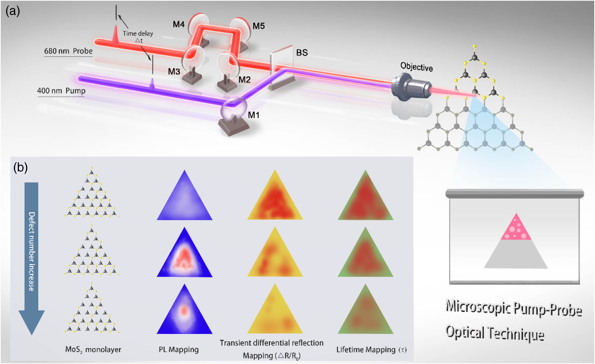
Figure 1.(a) Schematic of the experimental measurement by a microscopic pump-probe optical system. M1–M5 are the mirrors, and BS is the beam splitter. The wavelengths of the pump and probe are 400 nm and 680 nm, respectively. The time delay between the two laser pulses is controlled by the stepper motor. (b) Schematic of the dependence of PL mapping, transient differential reflection mapping, and lifetime mapping on the defect number for the same piece of monolayer based on the data in our work.
C. Basic Optical Properties Measurements
X-ray photoelectron spectroscopic profiles shown in Figs. 2(a) and 2(b) were measured by a Thermo Scientific ESCA Lab 250Xi XPS with a monochromatic K-alpha radiation (KR) Al X-ray line. The home-built optical system was also adapted to perform the measurements of reflectance spectra, PL spectra, and PL mapping images. Reflectance spectra were recorded by the spectrometer (Princeton Instruments SP2500) with a objective (Olympus MPlanFL, ). The relative reflectivity shown in reflectance spectra of Fig. 3(a) was obtained by dividing the reflected intensity of the sample to that of the substrate. The PL spectra shown in Fig. 3(b) and PL mapping images shown in Figs. 4(a)–4(c) were measured by the home-built optical system under the excitation conditions of a 400 nm laser with a pump fluence of at room temperature. The step size for the measurements of PL mapping is about 1 μm. The measurements of Raman spectra shown in Fig. 2(c) and PL mapping images shown in Fig. 5 were performed by a commercial confocal microscope (JY-HR800) under a 532 nm laser with a power of 50 mW at room temperature. The diameter of the laser spot is about 1 μm. The step size for the measurements of commercial PL mapping is about 0.5 μm.

Figure 2.(a) High-resolution XPS profiles for Mo 3d of with the in situ, first deal, and second deal samples. Blue and red lines represent the intrinsic () and defective (), respectively. (b) High-resolution XPS profiles for S 2p of with different deal times. (c) Raman spectra of the same piece of with in situ (gray), first deal (green), and second deal (blue) samples.
Figure 3.Optical properties of the same piece of with in situ (gray), first deal (green), and second deal (blue) samples are as follows: (a) reflectance spectra, (b) PL spectra, (c) transient differential reflection spectra. The sample is excited under a pump fluence of . The wavelengths of pump and probe are 400 nm and 680 nm, respectively. The inset image in (a) is the optical image of the measured monolayer, and the scale bar is 5 μm.
Figure 4.(a)–(c) are the PL mapping images of with in situ, first deal, and second deal samples. (d)–(f) are the peak mapping images of the corresponding samples. The measured sample is the same piece of monolayer.
Figure 5.(a)–(c) are the PL mapping images of a monolayer with the in situ, first deal, and second deal samples measured by commercial confocal microscope under a 532 nm laser with a power of 50 mW at room temperature. The inset image in (a) is the optical image of the corresponding monolayer, and the scale bar is 10 μm.
3. RESULTS AND DISCUSSION
In this work, a microscopic pump-probe optical system integrates multiple measuring functions including microscopic reflection, PL, signal-particle scattering, and femtosecond time-resolved spectra, which is used to characterize the defects of monolayer TMDs materials including and monolayers. As can be seen in Fig. 1(a), the pump and probe light beams passing through a microscopic system are collinearly focused on the surface of the sample, and then the laser beams begin to point-by-point scan the surface of the sample in the plane by using a 2D electronically controlled translating platform. Finally, the PL mapping, transient differential reflection mapping, and lifetime mapping can be achieved by this technique. More details of this microscopic pump-probe optical system can be found in the experiment section. As shown in Fig. 1(b), the same piece of monolayer is processed three times with different annealing conditions to increase the number of defects (seen in the experiment section). As shown in Fig. 1(b), the PL intensity of the sample does not increase or decrease monotonously as the defect number increases, which implies PL mapping cannot reflect the number of defects at each point. From the transient differential reflection mapping images, the results indicate that the intensity decreases monotonously when the defect number increases, which indicates that the distribution of defects can be visualized by the microscopic pump-probe technique. Moreover, through mapping the transient differential reflection spectra of the same piece of monolayer, it is found that there is a linear relationship between the transient differential reflection intensity and the defect density, suggesting that the defect number of each point of the sample can be further quantitatively estimated by using this technique. In addition, the lifetime resolution of each point of the sample can also be obtained by this technique.
The measurements of XPS were used to roughly characterize the increase of defect number as the number of times of annealing increases. As shown in Figs. 2(a) and 2(b), the sulfur vacancy concentration of the monolayer is overall increased. The XPS spectra of Mo 3d consisted of two sets of peaks that can be respectively assigned to intrinsic () and defective () in Fig. 2(a). The deconvoluted 3d5/2 and 3d3/2 doublet peaks depict the contributions of (doublets located at 232.88 eV and 229.70 eV) and (peaks at 232.52 eV and 229.40 eV). As the number of times of annealing increases, the contribution of the defect gradually increases, while the intrinsic component gradually decreases. This result shows that hydrogen annealing can produce sulfur vacancies in . In addition, the XPS spectra of S 2p verify this argument in Fig. 2(b). For XPS peak analysis and deconvolution, the software Avantage 4.15 was employed, where Voigt line shapes and an active Shirley background were used for peak fitting. The S/Mo ratios were determined from the integrated areas of the S 2p and Mo 3d peaks factored by their corresponding relative sensitive factors. The molar ratio of the two and Mo elements can be calculated as follows: , where represents the integrated areas of the S 2p and Mo 3d peaks of the intrinsic and is the sensitive factor of the corresponding element. The error in the S/Mo ratios was obtained from the peak fitting residuals given by the Avantage 4.15 software. The XPS results indicate that the values of the S:Mo ratio are 1.77 (in situ), 1.70 (first deal), and 1.66 (second deal), respectively. The corresponding average defect ratio of the whole sample is 11.5%, 15%, and 17%, respectively. This result indicates that the number of defects overall increases as the number of times of annealing increases. The increase of sulfur vacancy concentration of the sample is further demonstrated by the Raman spectra as shown in Fig. 2(c), which were measured by a commercial confocal microscope under 532 nm laser with a power of 50 mW at room temperature. The splitting between in-plane and out-of-plane Raman modes is that confirms the monolayer nature of . The peak of the monolayer shows a significant redshift as the sulfur vacancy concentration increases because sulfur vacancies are able to wrench the S-Mo bond to induce the lateral sliding of the top S layer. The continuous broadening and intensity attenuation of the and bands also reconfirm the growing loss of crystal symmetry.
This microscopic pump-probe system was used to measure the microscopic reflection, PL, and transient differential reflection spectra of the same sample as shown in Fig. 3. The reflectance spectra of the same piece of with the in situ sample (gray line), first deal sample (green line), and second deal sample (blue line) are presented in Fig. 3(a). It is seen that absorption peak positions of the monolayer are about 625 nm (B-exciton) and 670 nm (A-exciton), respectively [43], which remains substantially unchanged as the number of defects increases because the measurements of the static reflectance spectra represent the refractive index change of the whole monolayer. The increase of defect number has an insignificant effect on the refractive index of the whole sample, leading to the static reflectance spectra of the sample being insensitive to its defect number. Figure 3(b) presents the PL spectra of the monolayer with different defect numbers. For the measurements of PL spectra, a wavelength of 400 nm is used to excite the sample under a pump fluence of . As shown in Fig. 3(b), the PL peak position of monolayers on the substrate is at 679 nm, which has no change as the defect number increases, while the PL intensity of the sample first increases and then decreases as the defect number increases because the introduction of a small number of defects will reduce the formation of trions and the probability of exciton–exciton annihilation. The results lead to the increase of PL intensity after the first deal with the sample, while the PL intensity then reduces when the number of defects is further increased because the excessive increase of defects induces the reduction of exciton numbers [16].
Figure 3(c) shows the dependence of transient differential reflection () signals of the same sample on the delay time. The sample is excited under a pump fluence of . The wavelengths of pump and probe are 400 nm and 680 nm, respectively. As shown in Fig. 3(c), the peak intensity of the sample (, , and ) at the same point decreases from 1.98% to 0.66% as the defect number increases. The peak of the sample is dominated on the total number of excitons formed at the 0 ps point [44]. Therefore, it can be seen that the peak is dependent on the defect number because the existence of defects can modify the number of formed excitons at the initial time. From Fig. 3(c), it is also seen that the signals decay biexponentially. By using the biexponential function to fit the experimental data, the decay time constants of fast decay process and slow decay process () can be obtained. The are , , and , and the are , , and , respectively. The fast decay process includes exciton–exciton annihilation () and defect-assisted nonradiative recombination () [45,46]. It is seen that the process of exciton–exciton annihilation is dominant when the defect number is relatively small. The slow decay process mainly represents the radiative recombination lifetime of excitons in the monolayer [47–49].
To compare the ability to characterize defects between the micro-PL technique and the microscopic pump-probe technique, we used these two techniques to characterize the defects of on the micro-zone. As shown in Fig. 4, Figs. 4(a)–4(c) and Figs. 4(d)–4(f) are the PL mapping and peak mapping of the same monolayer with the increasing number of times of annealing, respectively. The measurements of the PL mapping of this sample were performed by a home-built optical system; the detailed measuring processes are shown in the experiment section. From the PL mapping images, on the whole, we can see that the PL intensity first increases and then decreases as the number of defects increases. The PL mapping images show that the PL intensity does not change monotonously with the increase of defect number, which indicates that there is no corresponding relationship between the PL intensity and the defect number. The reasons for this trend are explained forward. To the best of our knowledge, the PL mapping can only reflect the change of PL intensity at different points. However, there are many parameters that can largely affect the PL intensity of the monolayer, such as contact type between the monolayer and substrate, the surface states, and the number of defects. Even though we only add the number of defects (sulfur vacancies) in our measured samples, there is still no corresponding relationship between the PL intensity and the defect number because the PL mapping can only indicate there are different defect numbers at different points. This implies that it is unable to estimate whether the defect number of a point is more or less than that of another point, let alone quantifying the number of defects.
As shown in Fig. 4, it is seen that the variation trend of the peak mapping images is quite different from that of the PL mapping images. Since the differential reflection signal intensity is related to the exciton density that is dominant by the number of defects. Therefore, it is reasonable to infer that mapping the differential reflection signal intensities can identify the defect number of the monolayer at each point. As shown in Figs. 4(d)–4(f), we can see that the peak of the sample has an overall decrease and their peak intensities decrease monotonously at most points as the number of times of annealing increases. The result demonstrates that there must be a corresponding relationship between the peak intensity and the defect number. Generally, the pump-probe technique is based on the optical–optical double resonance. The pump light is usually used to excite carriers leading to the electrons’ transition to high energy state, and the probe light is used to monitor the evolution of carriers over time at a certain energy level (determined by the wavelength of the probe light). Through the pump-probe technique, we can get the differential reflection signals () of the monolayer TMD materials, where , and and are the reflection of probe light from the sample with and without the presence of pump light, respectively. For the monolayer TMD materials on the substrate, the reflection beam (probe light) is a superposition of three beams from the front surface and from the two interfaces. For the pump-probe measurements, the laser beams are under normal incidence, and the reflection coefficient of this multilayer system can be written as follows: where , , , , and . In these formulas, , are the complex indices of refraction for , , and Si, respectively. and are the thicknesses of the corresponding and layers, respectively. is the wavelength of probe light. The pump-injected carriers in the monolayer will change both the real part and the imaginary part of the index of refraction , where and are the real index of refraction and the absorption coefficient of the monolayer, respectively. According to Eq. (1), the reflection coefficient of the sample will be changed by the pump-injected carriers. The increase of the differential reflection signals indicates that the absorption of the monolayer is decreased by the pump-injected carriers due to the phase space filling effect of free carriers and excitons. More details can be found in these reports [47,50,51].
In order to further verify the experimental results and the reliability of our home-built optical system, we used a commercial confocal microscopy system to map the PL intensity of another monolayer that is dealt with in the same conditions as the preceding sample. Comparing the PL mapping images of Figs. 5(a)–5(c) with those of Figs. 4(a)–4(c), we can see that the change trend of PL intensity for both is consistent. The results indicate that the reliability of our system can be comparable to that of the commercial equipment. The precision of the PL mapping images measured by commercial devices is slightly higher than that measured by our home-built optical system. This is because the laser spot size and the accuracy of the scanning sample for our system are slightly weaker than that of commercial devices; this can be solved by improving the performance of the equipment in our system.
The peak mapping images have demonstrated that there is a corresponding relationship between the peak and the defect number. To estimate the defect number of the monolayer at each point, it is necessary to establish an accurate relationship between them. To achieve this goal, we first deduced the quantitative relationship between the peak and the saturation exciton density by measuring dependence of the differential reflection signal on the pump fluences. Figures 6(a)–6(c) show the pump-fluences-dependent differential reflection spectra at the same point of with in situ, first deal, and second deal samples. Because the exciton lifetime is much longer than the rising time, we can ignore the decay of the exciton density during the pump pulse. It is reasonable to assume that the exciton density at the peak time equals the injected carriers’ density. By substituting the pump power P (microwatt, µW), repetition frequency f (Hertz, Hz), and laser spot area S (centimeter squared, ) into the formula , we can get the energy density per unit area called the pump fluence J (microjoule per centimeter squared, ). From the pump fluence divided by the energy of a single photon hν (µJ), we can acquire the number of photons per unit area , and then we can estimate the injected exciton density () by using an absorption coefficient and a thickness for a monolayer and assuming that every pump photon absorbed by excites one exciton [47]. The peak signal intensity can be extracted from Figs. 6(a)–6(c), and then the injected exciton density dependence of peak is obtained as shown in Fig. 6(d). From Fig. 6(d), it is seen that the peak intensities of the differential reflection signal will reach their maximum as the pump-injected exciton density is increased. This is a saturated absorption effect that can be attributed to the reduction of the exciton transition strength by the pump-injected excitons and the pump-induced linewidth broadening of the excitons [44,52]. It is found that the measured data can be accurately described by a saturable absorption model , where , , and are the ratio coefficient, injected exciton density, and the saturation exciton density, respectively [44,47]. By using the formula above to fit the experimental data, we can get the values of for the same point of with different times of annealing, which are , , and , respectively.
Figure 6.(a)–(c) are the pump-fluences-dependent differential reflection spectra of the same point of . (d) is the dependence of peak on injected exciton density for the same point of with in situ (gray ball), first deal (green ball), and second deal (blue ball) samples. The solid lines (red) are the fitting curves. (e) is the dependence of saturation exciton density () on the peak of the same sample at different positions. Positions 1–4 are the ball, triangle, diamond, and hexagon, respectively. (f) is the dependence of defect ratio on the peak .
To find the corresponding relationship between the and the peak , we first measured the at four different positions for the same piece of . Then we extracted by fitting the experimental data and plotted a graph as shown in Fig. 6(e). It is seen that there is a linear relationship between the and the peak . This result indicates that we can acquire the of each point of monolayer through measuring its peak of the corresponding points under a certain pump fluence. Second, since the number of formed excitons excited by the pump light at the initial time is dominated by the defect number, it is reasonable to infer that there is a corresponding relationship between the defect ratio and . The exciton Bohr radius () in a monolayer is estimated to be 1–2 nm, which indicates that saturation exciton density is on the order of for a monolayer without any defects [53]. In our experiments, the measured maximum value of is about that is slightly lower than the theoretically estimated value. Therefore, it is rational to deduce that a point with a maximum measured value of has a defect ratio of 0. Finally, the of each point is divided by the maximum measured value of , and the dependence of the defect ratio on the peak can be obtained as shown in Fig. 6(f). It is worth noting that a point at a monolayer without any defects has a theoretical estimated of about , which corresponds to a sulfur atomic density of about . This result indicates that there is a proportional relationship between the defect density (sulfur vacancies) and the peak , suggesting that we can take advantage of the peak mapping to characterize the defect density of the sample. This suggests that the microscopic pump-probe technique is an effective and viable means to characterize the defect density of a monolayer on a micro-zone. In addition, there are various types of defects existing in monolayer TMD materials including domain walls, dislocations, strains, and impurities during the growth process. The microscopic pump-probe technique cannot be used to identify different types of defects that are also impossible to realize by using other optical measuring methods. In this work, the same piece of monolayer was annealed three times to increase the sulfur vacancies only. From the peak mapping images shown in Fig. 4, it is seen that the signal intensity changes of the in situ sample are not very large as a whole. It is reasonable to deduce that transient differential reflection signal intensity is more sensitive to the sulfur vacancies than other types of defects. The microscopic pump-probe technique used in this work to characterize one of the defect types (sulfur vacancies) has a certain value for the improvement of the growth quality and defect monitoring of TMDs materials. However, further research is also needed to study the effects of the defect types on the transient differential reflection intensity.
In order to prove the universality of this technique for TMD materials, we further mapped the transient differential reflection signals of a monolayer on a sapphire substrate to characterize its defect density as shown in Fig. 7. The measuring condition and process of is the same as that of , except the probe wavelength, which corresponds to its absorption peak position. The process of experimental data handling is the same as that before. We first mapped the peak of a monolayer as shown in Fig. 7(a), and then got the linear relationship between and peak as shown in Fig. 7(b). Finally, the defect density of the measured monolayer can be obtained according to the relationship between the defect ratio and peak deduced by previous measured results. For the monolayers, the proportional relationship between the defect density and the peak can be obtained to be about , which is the same as between different batches of the same TMD materials. For the monolayers, the proportional relationship between them is about , which is different from the value of the monolayers. Recently, other new 2D materials such as black phosphorus [54], MXene [55], and antimonene [56] have been developed that possess highly tunable and tailorable optoelectronic properties. These 2D materials, as the new members of the 2D materials family, have attracted considerable attention. It is reasonable to believe that this microscopic pump-probe technique may be also suitable for characterizing the defects of these 2D materials when their transient absorption strengths are dependent on the defect density. Further research is needed to resolve this important question.
Figure 7.(a) is a peak mapping image of monolayer with the in situ sample. The sample is excited under a pump fluence of . The wavelengths of pump and probe are 400 nm and 630 nm, respectively. (b) is the dependence of saturation exciton density () on the peak of the same piece of monolayer at different positions. The inset image in (b) is the optical image of the measured monolayer, and the scale bar is 5 μm.
Through transient differential reflection spectra, we can not only use their peak signal intensity to realize the characterization of the defect number but also get the resolution of the decay times of excitons in the monolayer on the micro-zone as shown in Fig. 8. The mapping images with the in situ, first deal, and second deal samples are shown in Figs. 8(a)–8(c). It is seen that the of the whole is overall increased as the defect number increases. The increase of is induced by the reduction of collision probability between excitons, which can be attributed to the increase of defect density that leads to the reduction of the exciton number. Figures 8(d)–8(f) show the mapping images of the sample with an increase in the number of times of annealing. We can see that of the whole is reduced from about 30 to 15 ps on the whole as the defect number increases. Since the increase of the defect number causes the faster relaxation of conduction-band electrons through defect-assistance nonradiative recombination that leads to the decrease of . This result further proves that the defect number of the monolayer is added with the increasing times of annealing. This result suggests that we can achieve the lifetime resolution of each point of the monolayer by the microscopic pump-probe technique. However, there are still some shortcomings of this microscopic pump-probe technique. Limited by the optical resolution and the numerical aperture of the objective lens, the spatial resolution of this system is on the order of several hundreds of nanometers. Meanwhile, because the system used a reflectance confocal microscope that is more sensitive to external vibration, it requires minimizing external disturbances as much as possible in the measurement process.
Figure 8.(a)–(c) are the decay time of fast decay process mapping images of the same piece of a monolayer with in situ, first deal, and second deal samples. (d)–(f) are the decay time of the slow decay process mapping images of the corresponding sample.
4. CONCLUSION
In summary, we proposed an effective method for microscopic characterization of the defects at each point of monolayer TMD materials. First, through mapping the transient differential reflection spectra of the same piece of monolayer with different defect numbers, it is found that the peak monotonously decreases when the defect number increases, while there is no monotonous relationship between the PL intensity and the defect number. The results indicate that there is a linear relationship between the peak and the defect density, which is universal for monolayer TMD materials. Second, by utilizing the linear relationship between them, the defect density of each point of monolayer TMDs can be further quantitatively estimated by using the microscopic pump-probe technique. Third, we can also achieve the lifetime resolution of each point of the sample on the micro-zone by this technique. From the results of decay time mapping, it is seen that the is increased and the is decreased as the defect number is increased, which further proves that the intensity of differential reflection signal is dominated by the number of defects. For 2D-materials-based optoelectronic devices, the control of defect density is crucial, which implies that visualizing the distribution of defects for 2D materials is necessary. This technique has the advantage of being time efficient, low cost, nondestructive, quantifiable, and compatible, which provides a way to improve the growth quality of 2D materials and the performance of 2D-materials-based devices.
Acknowledgment
Acknowledgment. X. W. and Y. Z. supervised the project. Y. Y. and Z. Z. built the optical system and performed the optical measuring experiments. X. Z. fabricated and characterized the basic properties of the samples. All the authors discussed the results and wrote the paper.
References
[1] F. N. Xia, H. Wang, D. Xiao, M. Dubey, A. Ramasubramaniam. Two-dimensional material nanophotonics. Nat. Photonics, 8, 899-907(2014).
[2] Q. H. Wang, K. Kalantar-Zadeh, A. Kis, J. N. Coleman, M. S. Strano. Electronics and optoelectronics of two-dimensional transition metal dichalcogenides. Nat. Nanotechnol., 7, 699-712(2012).
[3] Z. Wang, Z. Dong, Y. Gu, Y.-H. Chang, L. Zhang, L.-J. Li, W. Zhao, G. Eda, W. Zhang, G. Grinblat, S. A. Maier, J. K. W. Yang, C.-W. Qiu, A. T. S. Wee. Giant photoluminescence enhancement in tungsten-diselenide-gold plasmonic hybrid structures. Nat. Commun., 7, 11283(2016).
[4] B. Radisavljevic, A. Radenovic, J. Brivio, V. Giacometti, A. Kis. Single-layer MoS2 transistors. Nat. Nanotechnol., 6, 147-150(2011).
[5] W. Y. Wang, A. Klots, D. Prasai, Y. M. Yang, K. I. Bolotin, J. Valentine. Hot electron-based near-infrared photodetection using bilayer MoS2. Nano Lett., 15, 7440-7444(2015).
[6] F. H. L. Koppens, T. Mueller, P. Avouris, A. C. Ferrari, M. S. Vitiello, M. Polini. Photodetectors based on graphene, other two-dimensional materials and hybrid systems. Nat. Nanotechnol., 9, 780-793(2014).
[7] Y. Jiang, L. Miao, G. Jiang, Y. Chen, X. Qi, X.-F. Jiang, H. Zhang, S. Wen. Broadband and enhanced nonlinear optical response of MoS2/graphene nanocomposites for ultrafast photonics applications. Sci. Rep., 5, 16372(2015).
[8] D. H. Deng, K. S. Novoselov, Q. Fu, N. F. Zheng, Z. Q. Tian, X. H. Bao. Catalysis with two-dimensional materials and their heterostructures. Nat. Nanotechnol., 11, 218-230(2016).
[9] T. F. Jaramillo, K. P. Jørgensen, J. Bonde, J. H. Nielsen, S. Horch, I. Chorkendorff. Identification of active edge sites for electrochemical H2 evolution from MoS2 nanocatalysts. Science, 317, 100-102(2007).
[10] W. Zhou, X. L. Zou, S. Najmaei, Z. Liu, Y. M. Shi, J. Kong, J. Lou, P. M. Ajayan, B. I. Yakobson, J. C. Idrobo. Intrinsic structural defects in monolayer molybdenum disulfide. Nano Lett., 13, 2615-2622(2013).
[11] R. Addou, S. McDonnell, D. Barrera, Z. B. Guo, A. Azcatl, J. Wang, H. Zhu, C. L. Hinkle, M. Quevedo-Lopez, H. N. Alshareef, L. Colombo, J. W. P. Hsu, R. M. Wallace. Impurities and electronic property variations of natural MoS2 crystal surfaces. ACS Nano, 9, 9124-9133(2015).
[12] H. Li, C. Tsai, A. L. Koh, L. Cai, A. W. Contryman, A. H. Fragapane, J. H. Zhao, H. S. Han, H. C. Manoharan, F. Abild-Pedersen, J. K. Nørskov, X. L. Zheng. Activating and optimizing MoS2 basal planes for hydrogen evolution through the formation of strained sulphur vacancies. Nat. Mater., 15, 48-53(2016).
[13] G. López-Polín, C. Gómez-Navarro, V. Parente, F. Guinea, M. I. Katsnelson, F. Pérez-Murano, J. Gómez-Herrero. Increasing the elastic modulus of graphene by controlled defect creation. Nat. Phys., 11, 26-31(2014).
[14] H. Qiu, T. Xu, Z. L. Wang, W. Ren, H. Y. Nan, Z. H. Ni, Q. Chen, S. J. Yuan, F. Miao, F. Q. Song, G. Long, Y. Shi, L. T. Sun, J. L. Wang, X. R. Wang. Hopping transport through defect-induced localized states in molybdenum disulphide. Nat. Commun., 4, 2642(2013).
[15] Z. T. Wu, Z. Z. Luo, Y. T. Shen, W. W. Zhao, W. H. Wang, H. Y. Nan, X. T. Guo, L. T. Sun, X. R. Wang, Y. M. You, Z. H. Ni. Defects as a factor limiting carrier mobility in WSe2: a spectroscopic investigation. Nano Res., 9, 3622-3631(2016).
[16] H. Y. Nan, Z. L. Wang, W. H. Wang, Z. Liang, Y. Lu, Q. Chen, D. W. He, P. H. Tan, F. Miao, X. R. Wang, J. L. Wang, Z. H. Ni. Strong photoluminescence enhancement of MoS2 through defect engineering and oxygen bonding. ACS Nano, 8, 5738-5745(2014).
[17] X. K. Zhang, Q. L. Liao, S. Liu, Z. Kang, Z. Zhang, J. L. Du, F. Li, S. H. Zhang, J. K. Xiao, B. S. Liu, Y. Ou, X. Z. Liu, L. Gu, Y. Zhang. Poly(4-styrenesulfonate)-induced sulfur vacancy self-healing strategy for monolayer MoS2 homojunction photodiode. Nat. Commun., 8, 15881(2017).
[18] W. W. Zhao, Y. L. Wang, Z. T. Wu, W. H. Wang, K. D. Bi, Z. Liang, J. K. Yang, Y. F. Chen, Z. P. Xu, Z. H. Ni. Defect-engineered heat transport in graphene: a route to high efficient thermal rectification. Sci. Rep., 5, 11962(2015).
[19] A. McCreary, A. Berkdemir, J. Wang, M. A. Nguyen, A. L. Elías, N. Perea-López, K. Fujisawa, B. Kabius, V. Carozo, D. A. Cullen, T. E. Mallouk, J. Zhu, M. Terrones. Distinct photoluminescence and Raman spectroscopy signatures for identifying highly crystalline WS2 monolayers produced by different growth methods. J. Mater. Res., 31, 931-944(2016).
[20] J. Kibsgaard, Z. B. Chen, B. N. Reinecke, T. F. Jaramillo. Engineering the surface structure of MoS2 to preferentially expose active edge sites for electrocatalysis. Nat. Mater., 11, 963-969(2012).
[21] B. K. Erickson, R. Erni, Z. Lee, N. Alem, W. Gannett, A. Zettl. Determination of the local chemical structure of graphene oxide and reduced graphene oxide. Adv. Mater., 22, 4467-4472(2010).
[22] G. H. Lee, R. C. Cooper, S. J. An, S. Lee, A. van der Zande, N. Petrone, A. G. Hammerberg, C. Lee, B. Crawford, W. Oliver, J. W. Kysar, J. Hone. High-strength chemical-vapor-deposited graphene and grain boundaries. Science, 340, 1073-1076(2013).
[23] Y. H. Lee, X. Q. Zhang, W. J. Zhang, M. T. Chang, C. T. Lin, K. D. Chang, Y. C. Yu, J. T. Wang, C. S. Chang, L. J. Li, T. W. Lin. Synthesis of large-area MoS2 atomic layers with chemical vapor deposition. Adv. Mater., 24, 2320-2325(2012).
[24] Y. C. Lin, T. Bjorkman, H. P. Komsa, P. Y. Teng, C. H. Yeh, F. S. Huang, K. H. Lin, J. Jadczak, Y. S. Huang, P. W. Chiu, A. V. Krasheninnikov, K. Suenaga. Three-fold rotational defects in two-dimensional transition metal dichalcogenides. Nat. Commun., 6, 6736(2015).
[25] J. D. Fuhr, A. Saul, J. O. Sofo. Scanning tunneling microscopy chemical signature of point defects on the MoS2(0001) surface. Phys. Rev. Lett., 92, 026802(2004).
[26] D. W. Wang, K. H. Wu, I. R. Gentle, G. Q. Lu. Anodic chlorine/nitrogen co-doping of reduced graphene oxide films at room temperature. Carbon, 50, 3333-3341(2012).
[27] D. X. Yang, A. Velamakanni, G. Bozoklu, S. Park, M. Stoller, R. D. Piner, S. Stankovich, I. Jung, D. A. Field, C. A. Ventrice, R. S. Ruoff. Chemical analysis of graphene oxide films after heat and chemical treatments by X-ray photoelectron and micro-Raman spectroscopy. Carbon, 47, 145-152(2009).
[28] S. Mignuzzi, A. J. Pollard, N. Bonini, B. Brennan, I. S. Gilmore, M. A. Pimenta, D. Richards, D. Roy. Effect of disorder on Raman scattering of single-layer MoS2. Phys. Rev. B, 91, 195411(2015).
[29] A. C. Ferrari, D. M. Basko. Raman spectroscopy as a versatile tool for studying the properties of graphene. Nat. Nanotechnol., 8, 235-246(2013).
[30] A. C. Ferrari, J. C. Meyer, V. Scardaci, C. Casiraghi, M. Lazzeri, F. Mauri, S. Piscanec, D. Jiang, K. S. Novoselov, S. Roth, A. K. Geim. Raman spectrum of graphene and graphene layers. Phys. Rev. Lett., 97, 187401(2006).
[31] W. T. Su, N. Kumar, A. Krayev, M. Chaigneau. In situ topographical chemical and electrical imaging of carboxyl graphene oxide at the nanoscale. Nat. Commun., 9, 2891(2018).
[32] R. Beams, L. G. Cancado, A. Jorio, A. N. Vamivakas, L. Novotny. Tip-enhanced Raman mapping of local strain in graphene. Nanotechnology, 26, 175702(2015).
[33] S. Mignuzzi, N. Kumar, B. Brennan, I. S. Gilmore, D. Richards, A. J. Pollard, D. Roy. Probing individual point defects in graphene via near-field Raman scattering. Nanoscale, 7, 19413-19418(2015).
[34] A. M. van der Zande, P. Y. Huang, D. A. Chenet, T. C. Berkelbach, Y. M. You, G. H. Lee, T. F. Heinz, D. R. Reichman, D. A. Muller, J. C. Hone. Grains and grain boundaries in highly crystalline monolayer molybdenum disulphide. Nat. Mater., 12, 554-561(2013).
[35] H. R. Gutiérrez, N. Perea-Lopez, A. L. Elías, A. Berkdemir, B. Wang, R. Lv, F. Lopez-Urías, V. H. Crespi, H. Terrones, M. Terrones. Extraordinary room-temperature photoluminescence in triangular WS2 monolayers. Nano Lett., 13, 3447-3454(2013).
[36] Z. Liu, M. Amani, S. Najmaei, Q. Xu, X. L. Zou, W. Zhou, T. Yu, C. Y. Qiu, A. G. Birdwell, F. J. Crowne, R. Vajtai, B. I. Yakobson, Z. H. Xia, M. Dubey, P. M. Ajayan, J. Lou. Strain and structure heterogeneity in MoS2 atomic layers grown by chemical vapour deposition. Nat. Commun., 5, 5246(2014).
[37] W. Bao, M. Melli, N. Caselli, F. Riboli, D. S. Wiersma, M. Staffaroni, H. Choo, D. F. Ogletree, S. Aloni, J. Bokor, S. Cabrini, F. Intonti, M. B. Salmeron, E. Yablonovitch, P. J. Schuck, A. Weber-Bargioni. Mapping local charge recombination heterogeneity by multidimensional nanospectroscopic imaging. Science, 338, 1317-1321(2012).
[38] W. Bao, N. J. Borys, C. Ko, J. Suh, W. Fan, A. Thron, Y. J. Zhang, A. Buyanin, J. Zhang, S. Cabrini, P. D. Ashby, A. Weber-Bargioni, S. Tongay, S. Aloni, D. F. Ogletree, J. Q. Wu, M. B. Salmeron, P. J. Schuck. Visualizing nanoscale excitonic relaxation properties of disordered edges and grain boundaries in monolayer molybdenum disulfide. Nat. Commun., 6, 7993(2015).
[39] L. Wu, Y. Dong, J. Zhao, D. Ma, W. Huang, Y. Zhang, Y. Wang, X. Jiang, Y. Xiang, J. Li, Y. Feng, J. Xu, H. Zhang. Kerr nonlinearity in 2D graphdiyne for passive photonic diodes. Adv. Mater., 31, 1807981(2019).
[40] Z. Guo, H. Zhang, S. Lu, Z. Wang, S. Tang, J. Shao, Z. Sun, H. Xie, H. Wang, X. F. Yu. From black phosphorus to phosphorene: basic solvent exfoliation, evolution of Raman scattering, and applications to ultrafast photonics. Adv. Funct. Mater., 25, 6996-7002(2015).
[41] Z. Guo, S. Chen, Z. Wang, Z. Yang, F. Liu, Y. Xu, J. Wang, Y. Yi, H. Zhang, L. Liao. Metal‐ion‐modified black phosphorus with enhanced stability and transistor performance. Adv. Mater., 29, 1703811(2017).
[42] S. Tongay, J. Zhou, C. Ataca, J. Liu, J. S. Kang, T. S. Matthews, L. You, J. B. Li, J. C. Grossman, J. Q. Wu. Broad-range modulation of light emission in two-dimensional semiconductors by molecular physisorption gating. Nano Lett., 13, 2831-2836(2013).
[43] K. F. Mak, C. Lee, J. Hone, J. Shan, T. F. Heinz. Atomically thin MoS2: a new direct-gap semiconductor. Phys. Rev. Lett., 105, 136805(2010).
[44] N. Kumar, Q. N. Cui, F. Ceballos, D. W. He, Y. S. Wang, H. Zhao. Exciton-exciton annihilation in MoSe2 monolayers. Phys. Rev. B, 89, 125427(2014).
[45] D. Sun, Y. Rao, G. A. Reider, G. Chen, Y. M. You, L. Brezin, A. R. Harutyunyan, T. F. Heinz. Observation of rapid exciton-exciton annihilation in monolayer molybdenum disulfide. Nano Lett., 14, 5625-5629(2014).
[46] H. N. Wang, C. J. Zhang, F. Rana. Ultrafast dynamics of defect-assisted electron-hole recombination in monolayer MoS2. Nano Lett., 15, 339-345(2015).
[47] R. Wang, B. A. Ruzicka, N. Kumar, M. Z. Bellus, H.-Y. Chiu, H. Zhao. Ultrafast and spatially resolved studies of charge carriers in atomically thin molybdenum disulfide. Phys. Rev. B, 86, 045406(2012).
[48] T. Korn, S. Heydrich, M. Hirmer, J. Schmutzler, C. Schüller. Low-temperature photocarrier dynamics in monolayer MoS2. Appl. Phys. Lett., 99, 102109(2011).
[49] M. Palummo, M. Bernardi, J. C. Grossman. Exciton radiative lifetimes in two-dimensional transition metal dichalcogenides. Nano Lett., 15, 2794-2800(2015).
[50] L. Zhang, Z. Li, D. N. Basov, M. Fogler, Z. Hao, M. C. Martin. Determination of the electronic structure of bilayer graphene from infrared spectroscopy. Phys. Rev. B, 78, 235408(2008).
[51] A. Castellanos-Gomez, N. Agraït, G. Rubio-Bollinger. Optical identification of atomically thin dichalcogenide crystals. Appl. Phys. Lett., 96, 213116(2010).
[52] S. Sim, J. Park, J.-G. Song, C. In, Y.-S. Lee, H. Kim, H. Choi. Exciton dynamics in atomically thin MoS2: interexcitonic interaction and broadening kinetics. Phys. Rev. B, 88, 075434(2013).
[53] A. M. Jones, H. Yu, N. J. Ghimire, S. Wu, G. Aivazian, J. S. Ross, B. Zhao, J. Yan, D. G. Mandrus, D. Xiao, W. Yao, X. Xu. Optical generation of excitonic valley coherence in monolayer WSe2. Nat. Nanotechnol., 8, 634-638(2013).
[54] Y. Wang, F. Zhang, X. Tang, X. Chen, Y. Chen, W. Huang, Z. Liang, L. Wu, Y. Ge, Y. Song, J. Liu, D. Zhang, J. Li, H. Zhang. All-optical phosphorene phase modulator with enhanced stability under ambient conditions. Laser Photon. Rev., 12, 1800016(2018).
[55] X. Jiang, S. Liu, W. Liang, S. Luo, Z. He, Y. Ge, H. Wang, R. Cao, F. Zhang, Q. Wen, J. Li, Q. Bao, D. Fan, H. Zhang. Broadband nonlinear photonics in few-layer MXene Ti3C2Tx (T = F, O, or OH). Laser Photon. Rev., 12, 1700229(2018).
[56] Y. Wang, W. Huang, C. Wang, J. Guo, F. Zhang, Y. Song, Y. Ge, L. Wu, J. Liu, J. Li, H. Zhang. An all-optical, actively Q-switched fiber laser by an antimonene-based optical modulator. Laser Photon. Rev., 13, 1800313(2019).


