• Photonics Research
  • Vol. 7, Issue 7, 711 (2019)
Ying Yu1, Xiankun Zhang2, Zhangkai Zhou1, Zheng Zhang2, Yanjun Bao1, Haofei Xu1, Limin Lin1, Yue Zhang2、3、*, and Xuehua Wang1、4、*
Author Affiliations
  • 1State Key Laboratory of Optoelectronic Materials and Technologies, School of Physics, Sun Yat-sen University, Guangzhou 510275, China
  • 2State Key Laboratory for Advanced Metals and Materials, Beijing Municipal Key Laboratory for Advanced Energy Materials and Technologies, School of Materials Science and Engineering, University of Science and Technology Beijing, Beijing 100083, China
  • 3e-mail: yuezhang@ustb.edu.cn
  • 4e-mail: wangxueh@mail.sysu.edu.cn
  • show less
    DOI: 10.1364/PRJ.7.000711 Cite this Article Set citation alerts
    Ying Yu, Xiankun Zhang, Zhangkai Zhou, Zheng Zhang, Yanjun Bao, Haofei Xu, Limin Lin, Yue Zhang, Xuehua Wang. Microscopic pump-probe optical technique to characterize the defect of monolayer transition metal dichalcogenides[J]. Photonics Research, 2019, 7(7): 711 Copy Citation Text show less
    (a) Schematic of the experimental measurement by a microscopic pump-probe optical system. M1–M5 are the mirrors, and BS is the beam splitter. The wavelengths of the pump and probe are 400 nm and 680 nm, respectively. The time delay between the two laser pulses is controlled by the stepper motor. (b) Schematic of the dependence of PL mapping, transient differential reflection mapping, and lifetime mapping on the defect number for the same piece of MoS2 monolayer based on the data in our work.
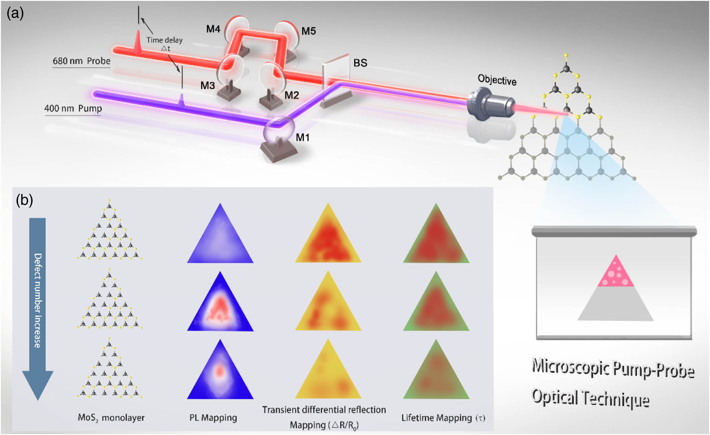
    Fig. 1. (a) Schematic of the experimental measurement by a microscopic pump-probe optical system. M1–M5 are the mirrors, and BS is the beam splitter. The wavelengths of the pump and probe are 400 nm and 680 nm, respectively. The time delay between the two laser pulses is controlled by the stepper motor. (b) Schematic of the dependence of PL mapping, transient differential reflection mapping, and lifetime mapping on the defect number for the same piece of MoS2 monolayer based on the data in our work.
    (a) High-resolution XPS profiles for Mo 3d of MoS2 with the in situ, first deal, and second deal samples. Blue and red lines represent the intrinsic MoS2 (i-MoS2) and defective MoS2 (d-MoS2), respectively. (b) High-resolution XPS profiles for S 2p of MoS2 with different deal times. (c) Raman spectra of the same piece of MoS2 with in situ (gray), first deal (green), and second deal (blue) samples.
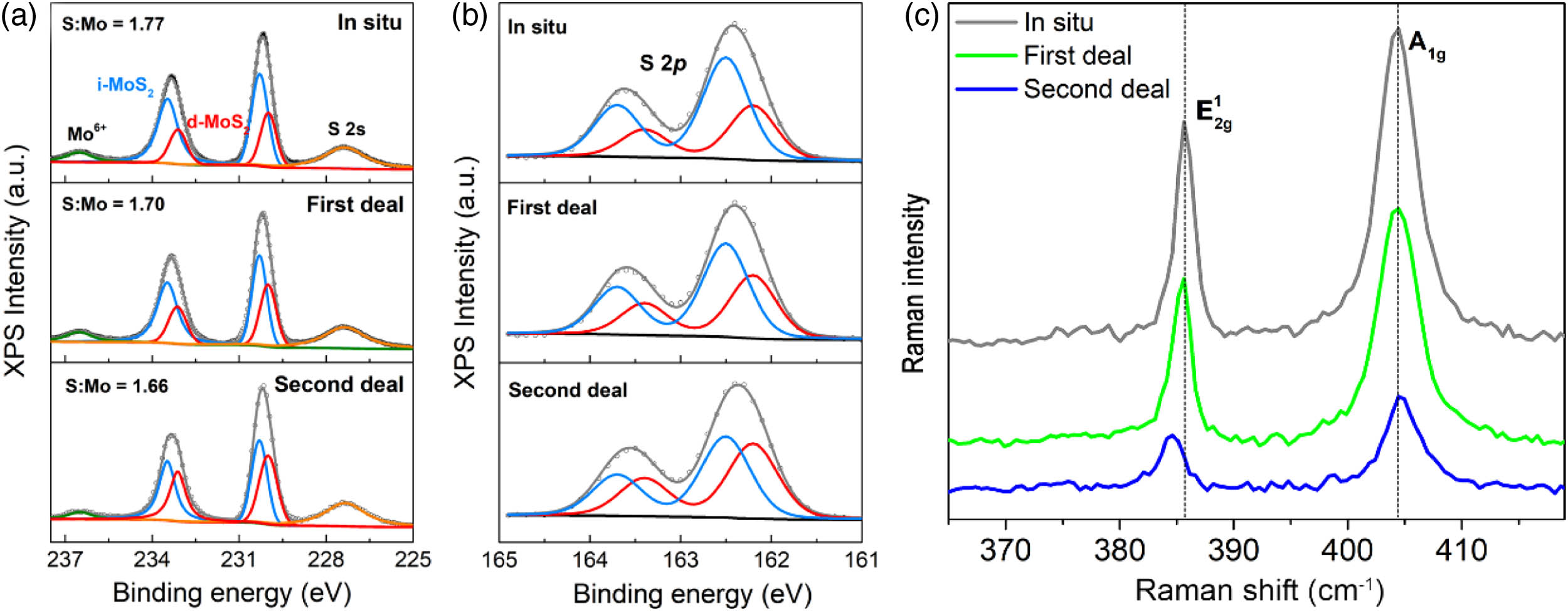
    Fig. 2. (a) High-resolution XPS profiles for Mo 3d of MoS2 with the in situ, first deal, and second deal samples. Blue and red lines represent the intrinsic MoS2 (i-MoS2) and defective MoS2 (d-MoS2), respectively. (b) High-resolution XPS profiles for S 2p of MoS2 with different deal times. (c) Raman spectra of the same piece of MoS2 with in situ (gray), first deal (green), and second deal (blue) samples.
    Optical properties of the same piece of MoS2 with in situ (gray), first deal (green), and second deal (blue) samples are as follows: (a) reflectance spectra, (b) PL spectra, (c) transient differential reflection spectra. The sample is excited under a pump fluence of 12.5 μJ/cm2. The wavelengths of pump and probe are 400 nm and 680 nm, respectively. The inset image in (a) is the optical image of the measured MoS2 monolayer, and the scale bar is 5 μm.
    Fig. 3. Optical properties of the same piece of MoS2 with in situ (gray), first deal (green), and second deal (blue) samples are as follows: (a) reflectance spectra, (b) PL spectra, (c) transient differential reflection spectra. The sample is excited under a pump fluence of 12.5  μJ/cm2. The wavelengths of pump and probe are 400 nm and 680 nm, respectively. The inset image in (a) is the optical image of the measured MoS2 monolayer, and the scale bar is 5 μm.
    (a)–(c) are the PL mapping images of MoS2 with in situ, first deal, and second deal samples. (d)–(f) are the peak ΔR/R0 mapping images of the corresponding samples. The measured sample is the same piece of MoS2 monolayer.
    Fig. 4. (a)–(c) are the PL mapping images of MoS2 with in situ, first deal, and second deal samples. (d)–(f) are the peak ΔR/R0 mapping images of the corresponding samples. The measured sample is the same piece of MoS2 monolayer.
    (a)–(c) are the PL mapping images of a MoS2 monolayer with the in situ, first deal, and second deal samples measured by commercial confocal microscope under a 532 nm laser with a power of 50 mW at room temperature. The inset image in (a) is the optical image of the corresponding MoS2 monolayer, and the scale bar is 10 μm.
    Fig. 5. (a)–(c) are the PL mapping images of a MoS2 monolayer with the in situ, first deal, and second deal samples measured by commercial confocal microscope under a 532 nm laser with a power of 50 mW at room temperature. The inset image in (a) is the optical image of the corresponding MoS2 monolayer, and the scale bar is 10 μm.
    (a)–(c) are the pump-fluences-dependent differential reflection spectra of the same point of MoS2. (d) is the dependence of peak ΔR/R0 on injected exciton density for the same point of MoS2 with in situ (gray ball), first deal (green ball), and second deal (blue ball) samples. The solid lines (red) are the fitting curves. (e) is the dependence of saturation exciton density (Ns) on the peak ΔR/R0 of the same sample at different positions. Positions 1–4 are the ball, triangle, diamond, and hexagon, respectively. (f) is the dependence of defect ratio on the peak ΔR/R0.
    Fig. 6. (a)–(c) are the pump-fluences-dependent differential reflection spectra of the same point of MoS2. (d) is the dependence of peak ΔR/R0 on injected exciton density for the same point of MoS2 with in situ (gray ball), first deal (green ball), and second deal (blue ball) samples. The solid lines (red) are the fitting curves. (e) is the dependence of saturation exciton density (Ns) on the peak ΔR/R0 of the same sample at different positions. Positions 1–4 are the ball, triangle, diamond, and hexagon, respectively. (f) is the dependence of defect ratio on the peak ΔR/R0.
    (a) is a peak ΔR/R0 mapping image of WS2 monolayer with the in situ sample. The sample is excited under a pump fluence of 12.5 μJ/cm2. The wavelengths of pump and probe are 400 nm and 630 nm, respectively. (b) is the dependence of saturation exciton density (Ns) on the peak ΔR/R0 of the same piece of WS2 monolayer at different positions. The inset image in (b) is the optical image of the measured WS2 monolayer, and the scale bar is 5 μm.
    Fig. 7. (a) is a peak ΔR/R0 mapping image of WS2 monolayer with the in situ sample. The sample is excited under a pump fluence of 12.5  μJ/cm2. The wavelengths of pump and probe are 400 nm and 630 nm, respectively. (b) is the dependence of saturation exciton density (Ns) on the peak ΔR/R0 of the same piece of WS2 monolayer at different positions. The inset image in (b) is the optical image of the measured WS2 monolayer, and the scale bar is 5 μm.
    (a)–(c) are the decay time of fast decay process (τfast) mapping images of the same piece of a MoS2 monolayer with in situ, first deal, and second deal samples. (d)–(f) are the decay time of the slow decay process (τslow) mapping images of the corresponding sample.
    Fig. 8. (a)–(c) are the decay time of fast decay process (τfast) mapping images of the same piece of a MoS2 monolayer with in situ, first deal, and second deal samples. (d)–(f) are the decay time of the slow decay process (τslow) mapping images of the corresponding sample.
    Ying Yu, Xiankun Zhang, Zhangkai Zhou, Zheng Zhang, Yanjun Bao, Haofei Xu, Limin Lin, Yue Zhang, Xuehua Wang. Microscopic pump-probe optical technique to characterize the defect of monolayer transition metal dichalcogenides[J]. Photonics Research, 2019, 7(7): 711
    Download Citation