[1] R. Soref. The past, present, and future of silicon photonics. IEEE J. Sel. Top. Quantum Electron., 12, 1678-1687(2006).
[2] A. Rahim, T. Spuesens, R. Baets, W. Bogaerts. Open-access silicon photonics: current status and emerging initiatives. Proc. IEEE, 106, 2313-2330(2018).
[3] M. Pantouvaki, P. D. Heyn, M. Rakowski, P. Verheyen, B. Snyder, S. A. Srinivasan, H. Chen, J. D. Coster, G. Lepage, P. Absil, J. V. Campenhout. 50 Gb/s silicon photonics platform for short-reach optical interconnects. Optical Fiber Communication Conference, Th4H.4(2016).
[4] A. E. Lim, J. Song, Q. Fang, C. Li, X. Tu, N. Duan, K. K. Chen, R. P. Tern, T. Liow. Review of silicon photonics foundry efforts. IEEE J. Sel. Top. Quantum Electron., 20, 405-416(2014).
[5] K. Giewont, K. Nummy, F. A. Anderson, J. Ayala, T. Barwicz, Y. Bian, K. K. Dezfulian, D. M. Gill, T. Houghton, S. Hu, B. Peng, M. Rakowski, S. Rauch, J. C. Rosenberg, A. Sahin, I. Stobert, A. Stricker. 300-mm monolithic silicon photonics foundry technology. IEEE J. Sel. Top. Quantum Electron., 25, 8200611(2019).
[6] F. Ottonello-Briano, C. Errando-Herranz, H. Rödjegård, H. Martin, H. Sohlström, K. B. Gylfason. Carbon dioxide absorption spectroscopy with a mid-infrared silicon photonic waveguide. Opt. Lett., 45, 109-112(2020).
[7] Y. Gao, P. Dong, Y. Shi, Y. Shi. Suspended slotted photonic crystal cavities for high-sensitivity refractive index sensing. Opt. Express, 28, 12272-12278(2020).
[8] K. De Vos, I. Bartolozzi, E. Schacht, P. Bienstman, R. Baets. Silicon-on-insulator microring resonator for sensitive and label-free biosensing. Opt. Express, 15, 7610-7615(2007).
[9] A. L. Washburn, R. C. Bailey. Photonics-on-a-chip: recent advances in integrated waveguides as enabling detection elements for real-world, lab-on-a-chip biosensing applications. Analyst, 136, 227-236(2010).
[10] L. Ren, X. Xu, S. Zhu, L. Shi, X. Zhang. Experimental realization of on-chip nonreciprocal transmission by using the mechanical Kerr effect. ACS Photon., 7, 2995-3002(2020).
[11] L. K. Chin, Y. Shi, A.-Q. Liu. Optical forces in silicon nanophotonics and optomechanical systems: science and applications. Adv. Devices Instrum., 2020, 1964015(2020).
[12] M. W. Pruessner, D. Park, T. H. Stievater, D. A. Kozak, W. S. Rabinovich. Optomechanical cavities for all-optical photothermal sensing. ACS Photon., 5, 3214-3221(2018).
[13] W. Bogaerts, H. Sattari, P. Edinger, A. Y. Takabayashi, I. Zand, X. Wang, A. Ribeiro, M. Jezzini, C. Errando-Herranz, G. Talli, K. Saurav, M. G. Porcel, P. Verheyen, B. Abasahl, F. Niklaus, N. Quack, K. B. Gylfason, P. O’Brien, U. Khan. MORPHIC: programmable photonic circuits enabled by silicon photonic MEMS. Proc. SPIE, 11285, 1128503(2020).
[14] S. Han, J. Beguelin, L. Ochikubo, J. Jacobs, T. J. Seok, K. Yu, N. Quack, C.-K. Kim, R. S. Muller, M. C. Wu. 32 × 32 silicon photonic MEMS switch with gap-adjustable directional couplers fabricated in commercial CMOS foundry. J. Opt. Microsyst., 1, 024003(2021).
[15] T. Nagai, K. Hane. Silicon photonic microelectromechanical switch using lateral adiabatic waveguide couplers. Opt. Express, 26, 33906-33917(2018).
[16] C. Errando-Herranz, A. Y. Takabayashi, P. Edinger, H. Sattari, K. B. Gylfason, N. Quack. MEMS for photonic integrated circuits. IEEE J. Sel. Top. Quantum Electron, 26, 8200916(2020).
[17] H. Sattari, A. Y. Takabayashi, P. Edinger, P. Verheyen, K. B. Gylfason, W. Bogaerts, N. Quack. Low-voltage silicon photonic MEMS switch with vertical actuation. IEEE 34th International Conference on Micro Electro Mechanical Systems (MEMS), 298-301(2021).
[18] P. Edinger, A. Y. Takabayashi, C. Errando-Herranz, U. Khan, H. Sattari, P. Verheyen, W. Bogaerts, N. Quack, K. B. Gylfason. Silicon photonic microelectromechanical phase shifters for scalable programmable photonics. Opt. Lett., 46, 5671-5674(2021).
[19] D. Y. Kim, Y. J. Park, D. U. Kim, M. S. Hong, A. Y. Takabayashi, Y. Jeong, J. Park, S. Han, N. Quack, K. Yu, S. Han. 16-core recirculating programmable Si photonic MEMS. Conference on Lasers and Electro-Optics, STh1Q.6(2021).
[20] K. Gilleo. Photonics challenge to electronic packaging. IEEE Trans. Compon. Packag. Technol., 24, 309-311(2001).
[21] S. Chinmoy, Z. Daming, L. Sheng. Simulating optoelectronics/MEMS hermetic packaging process with finite element method. Fifth International Conference on Electronic Packaging Technology Proceedings (ICEPT), 502-511(2003).
[22] H. Xia, M. N. Akram, E. Bardalen, A. Roy, K. E. Aasmundtveit, P. Ohlckers. Evaluation of silicon diaphragms for hermetic packaging of microbolometer arrays. IEEE 8th Electronics System-Integration Technology Conference (ESTC), 1-5(2020).
[23] F. Forsberg, A. Lapadatu, G. Kittilsland, S. Martinsen, N. Roxhed, A. C. Fischer, G. Stemme, B. Samel, P. Ericsson, N. Høivik, T. Bakke, M. Bring, T. Kvisterøy, A. Rør, F. Niklaus. CMOS-integrated Si/SiGe quantum-well infrared microbolometer focal plane arrays manufactured with very large-scale heterogeneous 3-D integration. IEEE J. Sel. Top. Quantum Electron., 21, 2700111(2015).
[24] T. Tekin. Review of packaging of optoelectronic, photonic, and MEMS components. IEEE J. Sel. Top. Quantum Electron., 17, 704-719(2011).
[25] A. Hilton, D. S. Temple. Wafer-level vacuum packaging of smart sensors. Sensors, 16, 1819(2016).
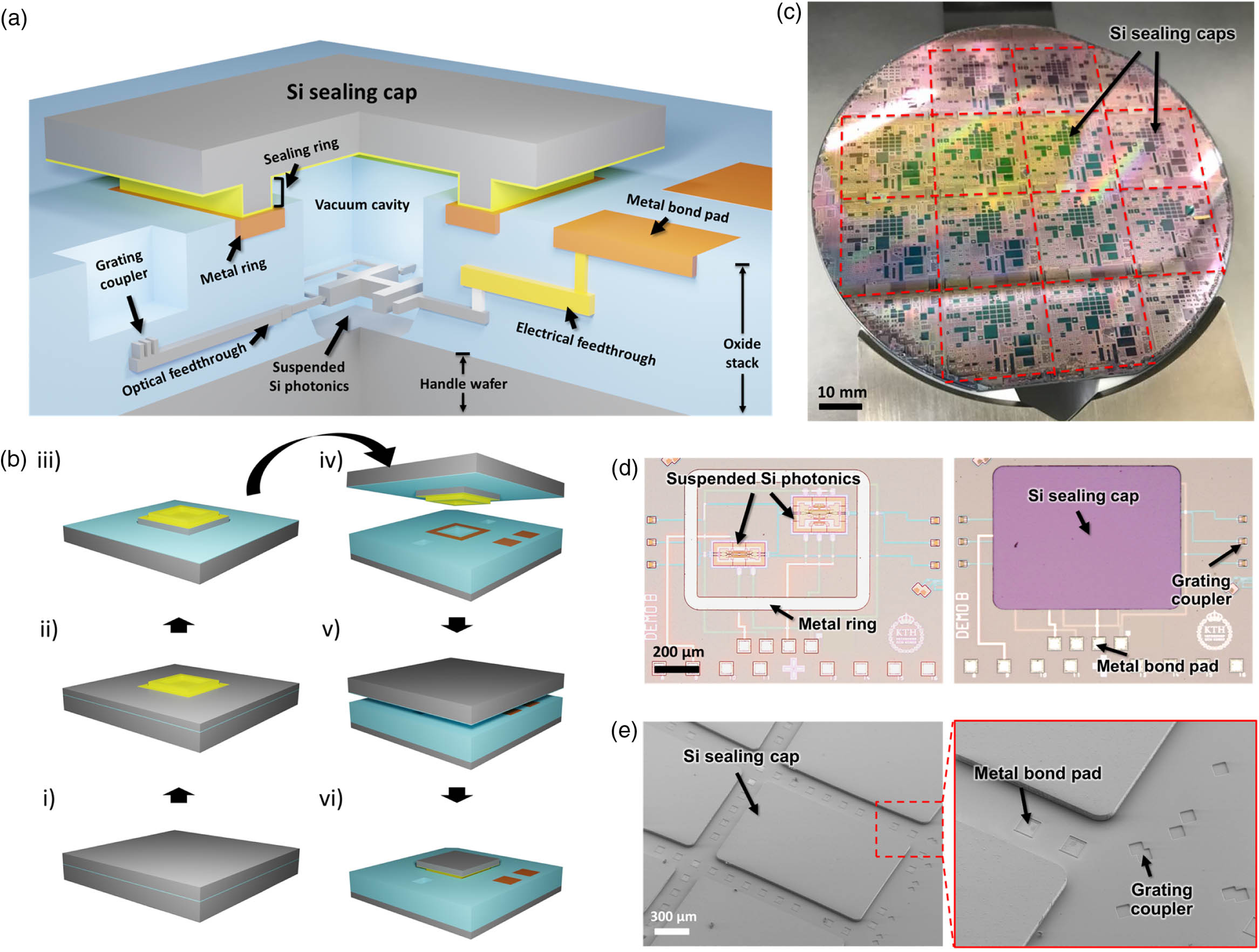
[26] X. Wang, S. J. Bleiker, P. Edinger, C. Errando-Herranz, N. Roxhed, G. Stemme, K. B. Gylfason, F. Niklaus. Wafer-level vacuum sealing by transfer bonding of silicon caps for small footprint and ultra-thin MEMS packages. J. Microelectromech. Syst., 28, 460-471(2019).
[27] S.-H. Lee, J. Mitchell, W. Welch, S. Lee, K. Najafi. Wafer-level vacuum/hermetic packaging technologies for MEMS. Proc. SPIE, 7592, 759205(2010).
[28] N. Pavarelli, J. S. Lee, M. Rensing, C. Scarcella, S. Zhou, P. Ossieur, P. A. O’Brien. Optical and electronic packaging processes for silicon photonic systems. J. Lightwave Technol., 33, 991-997(2015).
[29] L. Zimmermann, G. B. Preve, T. Tekin, T. Rosin, K. Landles. Packaging and assembly for integrated photonics—a review of the ePIXpack photonics packaging platform. IEEE J. Sel. Top. Quantum Electron., 17, 645-651(2011).
[30] K. Najafi. Micropackaging technologies for integrated microsystems: applications to MEMS and MOEMS. Proc. SPIE, 4979, 1-19(2003).
[31] P. D. John, H. Lau. 3D IC Integration and Packaging(2016).
[32] K. Zoschke, P. Mackowiak, K. Kröhnert, H. Oppermann, N. Jürgensen, M. Wietstruck, A. Göritz, S. Tolunay Wipf, M. Kaynak, K.-D. Lang. Cap fabrication and transfer bonding technology for hermetic and quasi hermetic wafer level MEMS packaging. IEEE 70th Electronic Components and Technology Conference (ECTC), 432-438(2020).
[33] G. Jo, P. Edinger, S. J. Bleiker, X. Wang, A. Y. Takabayashi, H. Sattari, N. Quack, M. Jezzini, P. Verheyen, G. Stemme, W. Bogaerts, K. B. Gylfason, F. Niklaus. Wafer-level vacuum sealing for packaging of silicon photonic MEMS. Proc. SPIE, 11691, 116910E(2021).
[34] M. Pantouvaki, S. A. Srinivasan, Y. Ban, P. D. Heyn, P. Verheyen, G. Lepage, H. Chen, J. D. Coster, N. Golshani, S. Balakrishnan, P. Absil, J. V. Campenhout. Active components for 50 Gb/s NRZ-OOK optical interconnects in a silicon photonics platform. J. Lightwave Technol., 35, 631-638(2017).
[35] N. Quack, H. Sattari, A. Y. Takabayashi, Y. Zhang, P. Verheyen, W. Bogaerts, P. Edinger, C. Errando-Herranz, K. B. Gylfason. MEMS-enabled silicon photonic integrated devices and circuits. IEEE J. Quantum Electron., 56, 8400210(2020).
[36] P. P. Absil, P. D. Heyn, H. Chen, P. Verheyen, G. Lepage, M. Pantouvaki, J. D. Coster, A. Khanna, Y. Drissi, D. V. Thourhout, J. V. Campenhout. IMEC iSiPP25G silicon photonics: a robust CMOS-based photonics technology platform. Proc. SPIE, 9367, 93670V(2015).
[37] D. Vermeulen, S. Selvaraja, P. Verheyen, G. Lepage, W. Bogaerts, P. Absil, D. V. Thourhout, G. Roelkens. High-efficiency fiber-to-chip grating couplers realized using an advanced CMOS-compatible silicon-on-insulator platform. Opt. Express, 18, 18278-18283(2010).