• Photonics Research
  • Vol. 10, Issue 2, A14 (2022)
Gaehun Jo1, Pierre Edinger1, Simon J. Bleiker1, Xiaojing Wang1, Alain Yuji Takabayashi2, Hamed Sattari2, Niels Quack2, Moises Jezzini3, Jun Su Lee3, Peter Verheyen4, Iman Zand5, Umar Khan5, Wim Bogaerts5, Göran Stemme1, Kristinn B. Gylfason1、6、*, and Frank Niklaus1、7、*
Author Affiliations
  • 1Division of Micro and Nanosystems, KTH Royal Institute of Technology, 11428 Stockholm, Sweden
  • 2École Polytechnique Fédérale de Lausanne (EPFL), 1015 Lausanne, Switzerland
  • 3Tyndall National Institute, Lee Maltings Complex Dyke Parade, T12 R5CP Cork, Ireland
  • 4imec vzw. 3DSIP Department, Si Photonics Group, Kapeldreef 75, 3001 Leuven, Belgium
  • 5Department of Information Technology, Photonics Research Group, Ghent University - IMEC, 9052 Gent, Belgium
  • 6e-mail: gylfason@kth.se
  • 7e-mail: frank@kth.se
  • show less
    DOI: 10.1364/PRJ.441215 Cite this Article Set citation alerts
    Gaehun Jo, Pierre Edinger, Simon J. Bleiker, Xiaojing Wang, Alain Yuji Takabayashi, Hamed Sattari, Niels Quack, Moises Jezzini, Jun Su Lee, Peter Verheyen, Iman Zand, Umar Khan, Wim Bogaerts, Göran Stemme, Kristinn B. Gylfason, Frank Niklaus. Wafer-level hermetically sealed silicon photonic MEMS[J]. Photonics Research, 2022, 10(2): A14 Copy Citation Text show less
    Wafer-level hermetic packaging of Si photonic MEMS. (a) Cut-away 3D illustration of a hermetically sealed suspended photonic MEMS device. (b) Process flow of the hermetic packaging approach by transfer bonding of a Si sealing cap: steps (i), (ii) patterning of sealing rings by deep reactive ion etching (DRIE) on the SOI cap wafer, followed by TiW/Au deposition and etching; (iii) etching of the sealing caps; (iv), (v) wafer alignment of the SOI wafer containing the caps and photonic device wafer, and bonding of the wafers inside a vacuum chamber at 250°C; (vi) removal of the Si handle (substrate) layer of the SOI cap wafer by DRIE such that only the thin vacuum sealing caps remain on the photonic device wafer. (c) Photograph of a full wafer with sealed Si photonic MEMS. (d) Microscope images before sealing (left) and after sealing (right). (e) SEM images of the bond pads and grating couplers around the thin sealing caps.
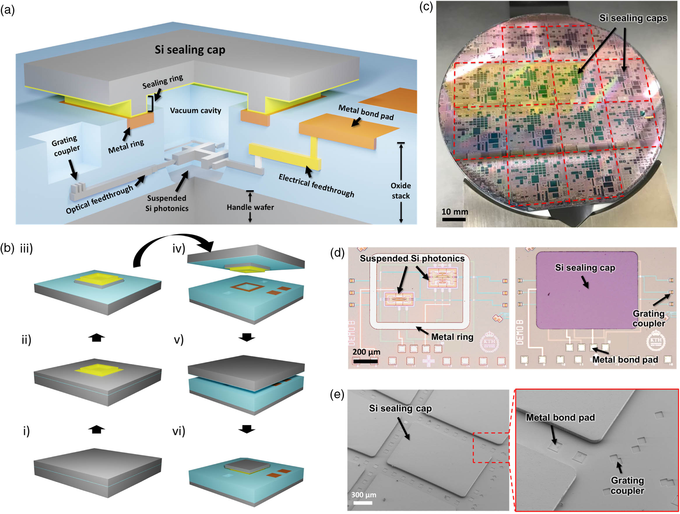
    Fig. 1. Wafer-level hermetic packaging of Si photonic MEMS. (a) Cut-away 3D illustration of a hermetically sealed suspended photonic MEMS device. (b) Process flow of the hermetic packaging approach by transfer bonding of a Si sealing cap: steps (i), (ii) patterning of sealing rings by deep reactive ion etching (DRIE) on the SOI cap wafer, followed by TiW/Au deposition and etching; (iii) etching of the sealing caps; (iv), (v) wafer alignment of the SOI wafer containing the caps and photonic device wafer, and bonding of the wafers inside a vacuum chamber at 250°C; (vi) removal of the Si handle (substrate) layer of the SOI cap wafer by DRIE such that only the thin vacuum sealing caps remain on the photonic device wafer. (c) Photograph of a full wafer with sealed Si photonic MEMS. (d) Microscope images before sealing (left) and after sealing (right). (e) SEM images of the bond pads and grating couplers around the thin sealing caps.
    Optical characterization of sealed Mach–Zehnder interferometers (MZIs) with suspended waveguide sections in one arm. (a) Split view of optical microscope images of four MZI devices before and after sealing within a rectangular cavity. (b) Example of measured optical transmission spectrum, along with the transmission spectrum of a reference grating-to-grating structure outside the sealed cavity. (c) Wafer map of the extinction ratio (ER) at a wavelength of 1550 nm of MZI devices placed on dies across the 100 mm wafer. An ER of 0 dB corresponds to collapsed waveguide sections. Four devices were measured on each die.
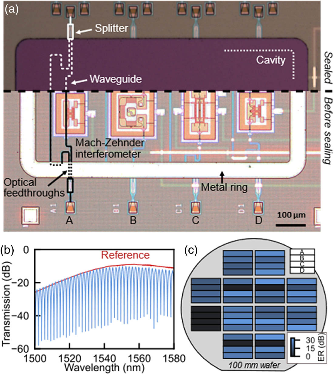
    Fig. 2. Optical characterization of sealed Mach–Zehnder interferometers (MZIs) with suspended waveguide sections in one arm. (a) Split view of optical microscope images of four MZI devices before and after sealing within a rectangular cavity. (b) Example of measured optical transmission spectrum, along with the transmission spectrum of a reference grating-to-grating structure outside the sealed cavity. (c) Wafer map of the extinction ratio (ER) at a wavelength of 1550 nm of MZI devices placed on dies across the 100 mm wafer. An ER of 0 dB corresponds to collapsed waveguide sections. Four devices were measured on each die.
    Effect of vacuum sealing on the performance of a Si photonic MEMS phase shifter. (a) Optical microscope image of the phase shifter before sealing. Inset: close-up of the suspended waveguide and movable actuator. (b) Phase shifter response in DC up to 36 V at a wavelength of 1550 nm, after sealing and dicing. (c), (d) Mechanical frequency response of the device before and after sealing, with (c) modulated output from the on-chip Mach–Zehnder interferometer and (d) mechanical phase offset with respect to the driving signal.
    Fig. 3. Effect of vacuum sealing on the performance of a Si photonic MEMS phase shifter. (a) Optical microscope image of the phase shifter before sealing. Inset: close-up of the suspended waveguide and movable actuator. (b) Phase shifter response in DC up to 36 V at a wavelength of 1550 nm, after sealing and dicing. (c), (d) Mechanical frequency response of the device before and after sealing, with (c) modulated output from the on-chip Mach–Zehnder interferometer and (d) mechanical phase offset with respect to the driving signal.
    White-light interferometry measurement of the deflection of a Si sealing cap. (a) Top view heatmap showing the deflection of a 25 μm thick Si cap with an area of 850 μm×1300 μm, resulting from the pressure difference between the inside and outside of the sealed cavity. (b) A cross section of (a) shows a maximum cap deflection of 0.63 μm at the center of the Si cap.
    Fig. 4. White-light interferometry measurement of the deflection of a Si sealing cap. (a) Top view heatmap showing the deflection of a 25 μm thick Si cap with an area of 850  μm×1300  μm, resulting from the pressure difference between the inside and outside of the sealed cavity. (b) A cross section of (a) shows a maximum cap deflection of 0.63 μm at the center of the Si cap.
    Donut-shaped sealed cavity with eight different electrical feedthrough test structures. The feedthroughs pass below the metal rings and connect a bond pad outside the cap with a bond pad in the center of the donut. Left: optical microscope image before sealing. Right: after sealing.
    Fig. 5. Donut-shaped sealed cavity with eight different electrical feedthrough test structures. The feedthroughs pass below the metal rings and connect a bond pad outside the cap with a bond pad in the center of the donut. Left: optical microscope image before sealing. Right: after sealing.
    Demonstration of flip-chip bonding of a chip with sealed photonic devices to a glass interposer. (a) Schematic cross section of a packaged Si photonic chip that is flip-chip bonded to a glass interposer. (b) Photograph of a packaged Si photonic chip that is flip-chip bonded to a glass interposer. (c) Photograph of the caps on top of the vacuum sealed cavities and Au/solder bumps that are visible through the glass interposer.
    Fig. 6. Demonstration of flip-chip bonding of a chip with sealed photonic devices to a glass interposer. (a) Schematic cross section of a packaged Si photonic chip that is flip-chip bonded to a glass interposer. (b) Photograph of a packaged Si photonic chip that is flip-chip bonded to a glass interposer. (c) Photograph of the caps on top of the vacuum sealed cavities and Au/solder bumps that are visible through the glass interposer.
    Gaehun Jo, Pierre Edinger, Simon J. Bleiker, Xiaojing Wang, Alain Yuji Takabayashi, Hamed Sattari, Niels Quack, Moises Jezzini, Jun Su Lee, Peter Verheyen, Iman Zand, Umar Khan, Wim Bogaerts, Göran Stemme, Kristinn B. Gylfason, Frank Niklaus. Wafer-level hermetically sealed silicon photonic MEMS[J]. Photonics Research, 2022, 10(2): A14
    Download Citation