Abstract
The plasma-enhanced chemical vapor deposition (PECVD) technique is well suited for fabricating optical filters with continuously variable refractive index profiles; however, it is not clear how the optical and structural properties of thin films differ when deposited on different substrates. Herein, silicon nitride films were deposited on silicon, fused silica, and glass substrates by PECVD, using silane and ammonia, to investigate the effects of the substrate used on the optical properties and structures of the films. All of the deposited films were amorphous. Further, the types and amounts of Si-centered tetrahedral Si–SivN4-v bonds formed were based upon the substrates used; Si–N4 bonds with higher elemental nitrogen content were formed on Si substrates, which lead to obtaining higher refractive indices, and the Si–SiN3 bonds were mainly formed on glass and fused silica substrates. The refractive indices of the films formed on the different substrates had a maximum difference of 0.05 (at 550 nm), the refractive index of SiNx films formed on silicon substrates was 1.83, and the refractive indices of films formed on glass were very close to those formed on fused silica. The deposition rates of these SiNx films are similar, and the extinction coefficients of all the films were lower than 10?4.Plasma-enhanced chemical vapor deposition (PECVD) is an excellent technique for fabricating antireflection films and optical filters. The PECVD technique can be used to prepare photoelectrical films of silicon nitride ()[1,2], silicon oxynitride[3,4], silicon carbonitride[5,6], and fluorinated silica[7,8]. These films are transparent in the visible (Vis) near-infrared region, exhibit good wear resistance, high stability, high surface hardness, and a high degree of densification, and thus are used in various applications[9–13]. The PECVD technique is currently one of the preferred deposition methods for the films due to a lower thermal budget than other chemical vapor deposition techniques, which are known as a low-temperature (lower than 400°C) deposition technique. Further, the dielectric constant[14] and chemical components[15,16] of the thus-deposited films can be controlled readily by adjusting the deposition parameters; the variable range of the refractive index is 1.83–2.06, and the extinction coefficient is lower than [17]. Therefore, the amorphous films were widely used in the field of optics; for instance, they can be used as optical waveguide materials in integrated optics[18], biorecognition layers of biosensors in biological applications[19], and antireflection films and passivation layers in photovoltaics for improving the photoelectric conversion efficiency[20]. More importantly, the adjustable refractive index[21], low-absorption, and amorphous state of the films make them particularly attractive for use as optical thin films, especially films that exhibit a gradient in their refractive index[22]. Thus, films, which can be considered as a tailored high refractive index structure, are expected to play a crucial role in many applications and devices.
For the advantages mentioned above, films deposited by the PECVD technique, were chosen as a high refractive index material to design and to deposit complex optical filters with a gradient refractive index profile, such as broadband antireflection filters, notch filters, and laser protection filters. Besides, films can be deposited on a Si substrate with nanostructures as an optical microstructure device to improve the imaging properties of the optical field. All of these applications are related to the effects of various substrates on films; this is why we need to do this study.
Several researchers have reported that the optical properties and microstructures of thin films are affected by the material properties of the substrate used[23–26]. For example, the radio frequency (RF) magnetron sputtering technique was used to synthesize indium gallium nitride (InGaN) crystalline films on n- and p-type Si substrates. It was found that the choice of the substrate material had a significant effect on the optical, morphological, and structural characteristics of the InGaN films[24]. Other researchers used the same method to deposit zinc oxide (ZnO) crystalline films onto Si, sapphire, polyethylene terephthalate (PET), and polypropylene carbonate substrates and found that the ZnO crystalline films formed on the PET substrates showed better optical and structural characteristics[25]. These reports suggest that the material properties of the substrate used affect those of the deposited thin films, including their optical characteristics and structures. However, few researchers have studied the influence of substrates on the optical properties of amorphous films deposited by PECVD at present. Therefore, to improve the manufacturing accuracy of optical films and to clarify the differences in the characteristics of the films deposited on various substrates, it is necessary to study the effects of various substrates on the optical and structural characteristics of films.
Sign up for Chinese Optics Letters TOC. Get the latest issue of Chinese Optics Letters delivered right to you!Sign up now
In this Letter, the films were deposited by the PECVD technique using silane () and ammonia () gases on Si, fused silica (FS), and glass substrates. The structural and optical properties of the films in the Vis near-infrared region were measured. We used the chemical bond configurations to analyze the changed refractive index of films. By analyzing these results, the effects of various substrates on the structural and optical properties of the films were clarified, which can be referenced by other researchers.
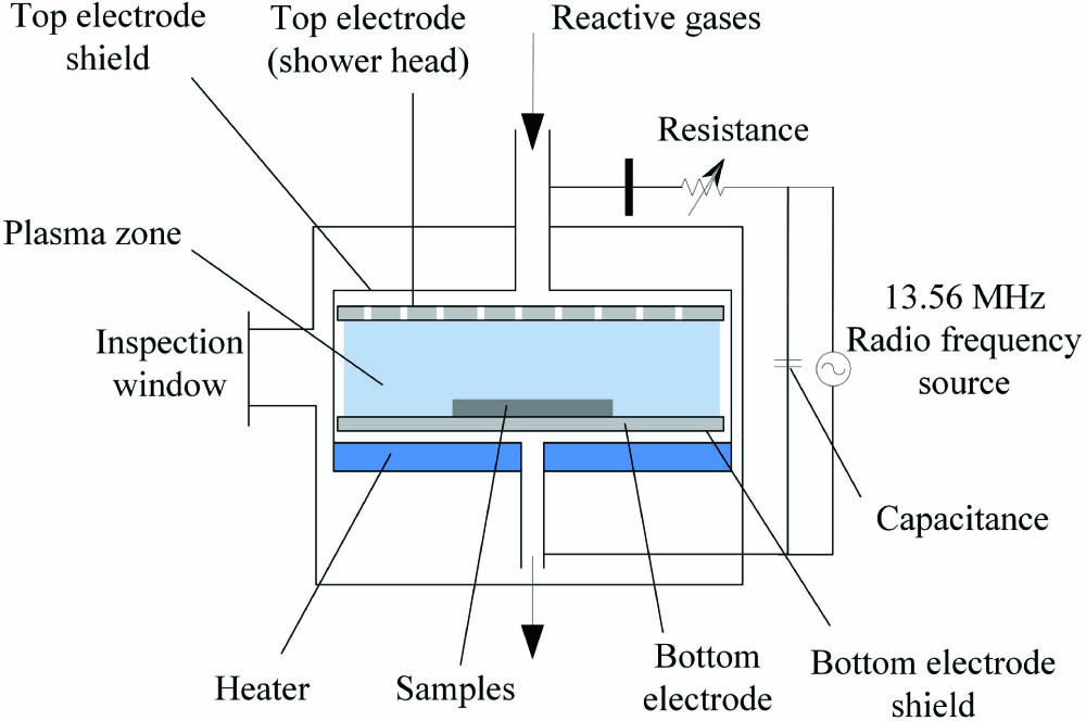
thin films were deposited by the RF-PECVD technique on a p-type crystalline (100) single-polished Si substrate with a thickness of 500 μm (), FS substrate with a thickness of 2 mm (), and glass substrate with a thickness of 1 mm (). All the experiments were performed in a class 1000 cleanroom. The substrates were cleaned with a mixture of ethanol and ether (3:1) and then heated for 10 min. Finally, the dried substrates were placed in the vacuum chamber of the coating system. The coating system used was a typical flat-plate PECVD (RF 13.56 MHz) system (PD-220 N™, SAMCO). The upper plate of the chamber had many holes with different sizes and is called the shower plate. All reactive gases were fully mixed through the shower plate before they entered the chamber. Figure 1 shows a schematic diagram of the RF-PECVD coating machine. Before the depositing process, the base pressure of the chamber was , and all the substrates were heated at least 40 min, which means that all the substrates were heated uniformly, avoiding the thermal gradient effects caused by the difference in the sample thickness. The films were deposited at a temperature of 250°C, chamber pressure of 100 Pa, deposition time of 6 min, and RF power of 200 W, and the flow rates of (10% in Ar) and (purity, 99.999%) were 60 sccm (standard cubic centimeters per minute). For convenience, the thin films formed at Si, glass, and FS substrates were named , , and , respectively.

Figure 1.Schematic of RF-PECVD coating system used in this study.
X-ray diffraction (XRD) using a diffractometer (Advance-D8, Bruker) equipped with a radiation source having was performed to determine the crystalline states of the films. The X-ray photoelectron spectroscopy (XPS) (K-Alpha, Thermo Fisher) was used to analyze the relative atomic composition and the chemical bonding configuration formed within the various films. XPS measurements were performed using monochromatized X rays from an source (1486.6 eV). The sample surface was etched using a 2 keV Ar ion beam with a current of 10 mA applied for 30 s. The spectra were analyzed and processed using the Thermo Avantage software. All the XPS spectra were corrected for any charging effects by fixing the C 1s binding energy (BE) at 284.8 eV and were subjected to Shirley background subtraction. The experimental data were evaluated using the Powell fitting algorithm and Gauss–Lorentz peak shape. The BE scale was referenced from the BE database, which can provide enough information about the chemical composition of the samples.
An ultraviolet (UV)-Vis spectrophotometer (Lambda 950, Perkin Elmer) was used to measure the transmittances of the films formed on the glass and FS substrates. The refractive indices, extinction coefficients, and physical thicknesses of the films were determined from a spectroscopic ellipsometer (M-2000UI, J. A. Woollam) using the Cauchy model. The optical film design software TFCalc was used to establish the “air/films/substrate/air” model for fitting the transmittance values of the thin films formed on Si substrates.
The XRD patterns of the non-stoichiometric thin films formed on different substrates are shown in Figs. 2(a) and 2(b). Figure 2(a) shows the XRD patterns of the thin films formed on the -type crystalline (100) single-polished Si substrates. It can be seen that all the samples exhibit a strong peak at the same value. However, this peak is not attributable to the films but is related to the Si substrate (100) itself. Figure 2(b) shows the XRD patterns of the thin films formed on the glass and FS substrates. No peak related to a crystal plane was observed; this was in keeping with previous reports[27]. In addition, it is known that as-deposited PECVD films often contain substantial amounts of bonded hydrogen, and that these films are more properly described as hydrogenated films[28,29]. In this regard, PECVD films are both structurally undefined (amorphous) and chemically undefined (non-stoichiometric)[2,30,31]. Therefore, it is confirmed that the films deposited on all three substrates were amorphous.
Figure 2.XRD patterns of thin films formed by PECVD method on (a) Si and (b) glass and fused silica (FS).
Table 1 shows the relative atomic concentrations of elemental Si and N in the films. The concentrations are the semi-quantitative test results; the uncertainty is for XPS results because of some variations in the composition depending on the depth of the analysis within the layer. It can be found that the relative atomic concentrations of Si and N of all the films are similar, and the concentration of elemental Si in the is slightly higher than that of other elements.
| Samples | Silicon (%) | Nitrogen (%) | Uncertainty (%) |
|---|
| SiNx1 | 48 | 52 | ±4 |
| SiNx2 | 46 | 54 | ±4 |
| SiNx3 | 46 | 54 | ±4 |
Table 1. Relative Atomic Concentrations of Si and N of Films Deposited on Various Substrates, Obtained by XPS
In order to analyze the chemical bond configurations of amorphous and non-stoichiometric films, two models are commonly used to describe the bonds: random bonding model (RBM) and random mixture model (RMM). RBM and RMM are based on the Si-centered tetrahedrons with in-plane triply coordinated N as bonding structures[32].
Figures 3(a) and 3(b) are the Si and N 1s high-resolution XPS spectra of the films, respectively, and G represents the glass substrate. Figure 3(a) shows the BE values of the Si main peaks for all the films are greater than that for Si (99.60 eV)[33] and less than that for (102.40 eV)[34], which means the Si–N chemical bond configurations with different types and amounts of Si-centered tetrahedron bonds were formed inside the films[35]. The XPS Si spectra do not exhibit a low-energy peak near 99.60 eV related to elemental Si, suggesting that no Si–Si bonds or Si clusters were formed in these films. Besides, the results in Fig. 3(a) show that the BE value of the Si main peak of the films deposited on the Si, FS, and glass substrates decreased gradually from 101.90 eV to 101.70 eV, indicating that the relative concentration of elemental N in the films was higher than that in other films[36]. Figure 3(b) shows that the BE values of elemental N 1s main peaks for all the films varied from 397.50 eV to 397.86 eV, which correspond to the BE values for different non-stoichiometric films[37]. The atomic-level non-equilibrium mixtures were generated in the plasma of the reactive gas during the deposition process, further, in order to determine the types of the Si–N bonds formed in the samples, the typical Si-centered tetrahedron (, 1, 2, 3, 4) bond configurations were used for analysis. The chemical bond configurations based on Si-centered tetrahedrons were most likely to be formed inside the films that are shown in Table 2[32,38].
Figure 3.High-resolution XPS spectra of films formed on Si, glass (G), and FS substrates: (a) Si 2p spectra; (b) N 1s spectra.
| No. | Tetrahedron | Bonding Unit | EBa (eV) of Si 2p |
|---|
| 1 | Si–Si3N | Si3N | 100.30 |
| 2 | Si–Si2N2 | Si3N2 | 101.00 |
| 3 | Si–SiN3 | SiN | 101.70 |
| 4 | Si–N4 | Si3N4 | 102.40 |
Table 2. Binding Energies of All the Possible Chemical Bonds in Regions Si
Figure 3(a) shows that the main compounds of the films formed on FS, glass, and Si substrates were gradually changed from SiN (101.70 eV) to (102.40 eV). The BE values of two subpeaks in Si high-resolution spectra of the films were 101.30 eV () and 102.34 eV (). For the and films, the BE values of two subpeaks were 101.30 eV (), 102.10 eV (), 100.60 eV (), and 101.90 eV (). It is indicated that more , , and bonds were formed in the and films, while the bonds were formed in the films. In addition, the BE values of the two subpeaks in the films deposited on FS substrates are smallest, indicating that the Si-centered tetrahedral bonds with higher Si concentration were formed in the films.
The XPS results show that various Si-centered tetrahedral bonds were formed by the elemental Si and N in the films, which corresponded to various compounds (i.e., for and for SiN). Different compounds exhibit different dielectric constants and densities. As a result, the refractive indices and film thicknesses of the films were different. Compared with the and films deposited on the glass and FS substrates, the films deposited on the Si substrates displayed Si-centered tetrahedral structures with a higher N content, because of which their properties were similar to those of films. This meant that, under the deposition parameters, the refractive index of the films formed on the Si substrates was greater than those of the films formed on the FS and glass substrates; Ref. [39] shows the same results.
Image Infomation Is Not Enable
Figure 5.Deposition rates and physical thicknesses of films deposited on various substrates.
Figure 6.Transmittances of films: (a) on glass; (b) on FS.
Figure 6 shows the measured transmittance spectra of the substrates and films coincided at wavelengths that are integer multiples of , where is the reference wavelength, indicating that the films formed on the glass and FS substrates did not exhibit absorption[43]. This was consistent with the fact that the extinction coefficients of the films were close to zero. In addition, comparing with the measured transmittance, the calculated transmittance [Simulated (Si)] was shifted slightly. This was mainly owing to the fact that the film thickness of the films formed on various substrates was different; further, the depths of valleys differed due to the differences in the refractive indices. The transmittance deviation of the single-layer film is greater than 1% at the minimum point, which has obviously exceeded the accuracy of the spectrophotometer ().
In summary, films were deposited by the PECVD technique on Si, glass, and FS substrates. The analyses of the structures of the films showed that all the deposited films were amorphous. Si-centered tetrahedral bonds were formed in the films, and the bonds forming in films deposited on the crystalline Si substrates, while the , , and bonds formed in films deposited on the amorphous substrates (glass and FS). The optical properties of the films showed that the films have the maximum refractive indices (i.e., at 550 nm) in the range of 400–1100 nm, and the films have the lower refractive indices (i.e., at 550 nm). All of the films displayed the properties of low absorption (the extinction coefficients are lower than ). These substrates have less effect on the deposition rates of the films.
The PECVD technique is suitable for fabricating amorphous films that show extremely low absorption in the Vis to near-infrared region. In this study, the types and amounts of chemical bond configurations in the films were affected by the various substrates, which leads to the differences in the refractive indices. Thus, before designing and fabricating optical multilayer filters and devices, the effects of various substrate materials on structural and optical properties of amorphous films should be paid attention.
Further work is to study the effects of various deposition parameters on the structural and optical properties of films, such as reactive gas flow rates and temperatures.
References
[1] B. Karunagaran, S. J. Chung, S. Velumani, E.-K. Suh. Mater. Chem. Phys., 106, 130(2007).
[2] J. Jaglarz, M. Jurzecka-Szymacha, S. Kluska. Thin Solid Films, 669, 564(2019).
[3] A. E. T. Kuiper, S. W. Koo, F. H. P. M. Habraken, Y. Tamminga. J. Vac. Sci. Technol. B, 1, 62(1983).
[4] J. Dupuis, E. Fourmond, J. F. Lelièvre, D. Ballutaud, M. Lemiti. Thin Solid Films, 516, 6954(2008).
[5] C. Huber, B. Stein, H. Kalt. Thin Solid Films, 634, 66(2017).
[6] K. Olesko, H. Szymanowski, M. Gazicki-lipman, J. Balcerzak, W. Szymanski, W. Pawlak, A. Sobczyk-guzenda. Mater. Sci. Poland, 36, 56(2018).
[7] M. D. Barankin, T. S. Williams, E. Gonzalez, R. F. Hicks. Thin Solid Films, 519, 1307(2010).
[8] M. Abbasi-Firouzjah, B. Shokri. J. Appl. Phys., 114, 214102(2013).
[9] V. Cech, J. Studynka, B. Cechalova, J. Mistrik, J. Zemek. Surf. Coat. Tech., 202, 5572(2008).
[10] A. Upadhyaya, M. Sheoran, A. Rohatgi, 1273(2005).
[11] T. Lauinger, J. Schmidt, A. G. Aberle, R. Hezel. Appl. Phys. Lett., 68, 1232(1996).
[12] A. del Prado, E. San Andrés, F. L. Martinez, I. Mártil, G. González-Daz, W. Bohne, J. Röhrich, B. Selle, M. Fernández. Vacuum, 67, 507(2002).
[13] I. Koirala, C. Park, S. Lee, D. Choi. Chin. Opt. Lett., 17, 082301(2019).
[14] B. Rangarajan, A. Y. Kovalgin, K. Wörhoff, J. Schmitz. Opt. Lett., 38, 941(2013).
[15] M. F. Ceiler, P. A. Kohl, S. A. Bidstrup. J. Electrochem. Soc., 142, 2067(1995).
[16] I. Guler. Mater. Sci. Eng. B-Adv., 246, 21(2019).
[17] J. Xue, L. Hang, H. Liu. Opt. Tech, 40, 353(2014).
[18] J. Dupuis, E. Fourmond, D. Ballutaud, N. Bererd, M. Lemiti. Thin Solid Films, 519, 1325(2010).
[19] J. Seiffe, L. Weiss, M. Hofmann, L. Gautero, J. Rentsch(2008).
[20] P. Li, L. Hang, J. Xu, L. Li. J. Appl. Opt, 36, 206(2015).
[21] W. Jiang, D. Xu, B. Xiong, Y. Wang. Ceram. Int., 42, 1217(2016).
[22] L. Hang, W. Liu, L. Hang, S. Zhou. Laser & Optoelectron. Progress, 57, 130003(2020).
[23] A. Basak, A. Hati, A. Mondal, U. P. Singh, S. K. Taheruddin. Thin Solid Films, 645, 97(2018).
[24] E. Erdoğan, M. Kundakçı. Microelectron. Eng., 207, 15(2019).
[25] S. H. Ribut, C. A. C. Abdullah, M. Z. M. Yusoff. Results Phys., 13, 102146(2019).
[26] T. Jiang, R. Miao, J. Zhao, Z. Xu, T. Zhou, K. Wei, J. You, X. Zheng, Z. Wang, X. Cheng. Chin. Opt. Lett., 17, 020005(2019).
[27] B. Astinchap, K. G. Laelabadi. J. Phys. Chem. Solids, 129, 217(2019).
[28] W. A. Lanford, M. J. Rand. J. Appl. Phys., 49, 2473(1978).
[29] G. Santana, J. Fandino, A. Ortiz, J. C. Alonso. J. Non-Cryst. Solids, 351, 922(2005).
[30] W. R. Knolle, J. W. Osenbach. J. Appl. Phys., 58, 1248(1985).
[31] J. Thurn, R. F. Cook, M. Kamarajugadda, S. P. Bozeman, L. C. Stearns. J. Appl. Phys., 95, 967(2004).
[32] P. Cova, S. Poulin, O. Grenier, R. A. Masut. J. Appl. Phys., 97, 073518(2005).
[33] P. J. W. Weijs, J. F. van Acker, J. C. Fuggle, P. A. M. van der Heide, H. Haak, K. Horn. Surf. Sci., 260, 102(1992).
[34] G. M. Ingo, N. Zacchetti, D. della Sala, C. Coluzza. J. Vac. Sci. Tech. A, 7, 3048(1989).
[35] V. A. Gritsenko, R. W. N. Kowk, H. Wong, J. B. Xu. J. Non-Cryst. Solids, 297, 96(2002).
[36] S. Naskar, S. D. Wolter, C. A. Bower, B. R. Stoner, J. T. Glass. Appl. Phys. Lett., 87, 261907(2005).
[37] J. R. Shallenberger, D. A. Cole, S. W. Novak. J. Vac. Sci. Tech. A, 17, 1086(1999).
[38] N. Jehanathan, Y. Liu, B. Walmsley, J. Dell, M. Saunders. J. Appl. Phys., 100, 123516(2006).
[39] X. Zhang. Research on anti-reflection coatings by PECVD technology(2010).
[40] T. Begou, H. Krol, D. Stojcevski, F. Lemarchand, M. Lequime, C. Grezes-Besset, J. Lumeau. CEAS Space J., 9, 441(2017).
[41] K. Hendrix. Appl. Opt., 56, C201(2017).
[42] H. Liu, L. Hang, J. Xue. Opt. Instrum., 36, 364(2014).
[43] H. A. Macleod. Thin-Film Optical Filters(2018).