Qi Liu, Seeram Ramakrishna, Yun-Ze Long. Electrospun flexible sensor[J]. Journal of Semiconductors, 2019, 40(11): 111603
Search by keywords or author
- Journal of Semiconductors
- Vol. 40, Issue 11, 111603 (2019)
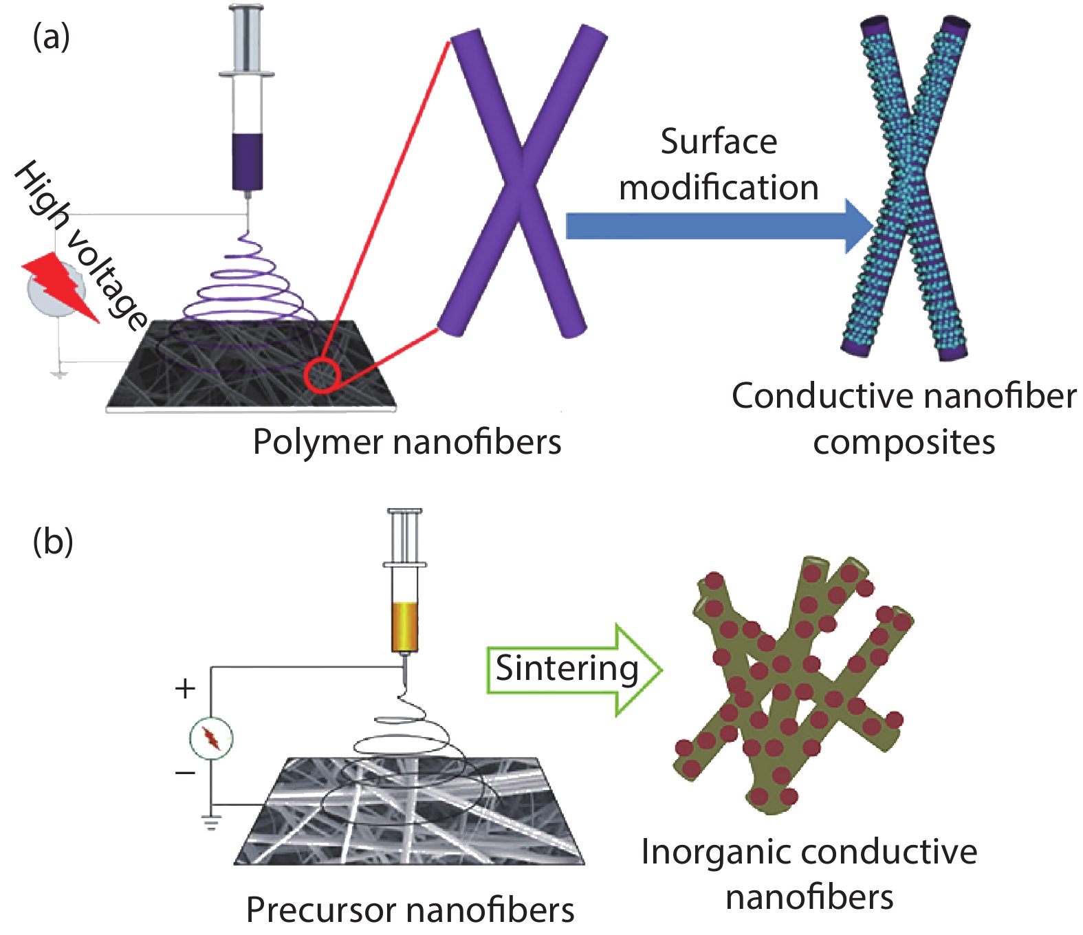
![(Color online) (a) Flowchart for preparing conductive nanofibers by surface modification[18]. (b) Flowchart for preparing conductive nanofibers by heat treatment[17].](/richHtml/jos/2019/40/11/111603/img_1.jpg)
Fig. 1. (Color online) (a) Flowchart for preparing conductive nanofibers by surface modification[18 ]. (b) Flowchart for preparing conductive nanofibers by heat treatment[17 ].
![(Color online) (a) Schematic diagram of field effect test device for zinc oxide fiber. (b) Field effect characteristics of Ce-doped ZnO[21]. (c) I–V curve of La-doped ZnO at different irradiation intensities. (d) Field effect characteristics of La-doped ZnO[19].](/richHtml/jos/2019/40/11/111603/img_2.jpg)
Fig. 2. (Color online) (a) Schematic diagram of field effect test device for zinc oxide fiber. (b) Field effect characteristics of Ce-doped ZnO[21 ]. (c) I –V curve of La-doped ZnO at different irradiation intensities. (d) Field effect characteristics of La-doped ZnO[19 ].
Fig. 3. (Color online) (a) Schematic of the printing unit. (b) Time-domain optical response of the ZnO fiber array. (c) I –V curve of the ZnO fiber array. (d) Flexible photodetector. (e) Optical photo of the nanowire array and silver electrode with a scale of 30 microns[22 ].
Fig. 4. (Color online) (a) I –V curves for PANI/TPU sensors under different tensions. (b) Responses when fingers are bent[24 ]. (c–f) Fibers with different patterned collectors[25 ].
Fig. 5. (Color online) (a) Electrical performance of the sensor at different pressures. (b) Current change of the sensor at different pressures. (c) Response of the sensor to human respiration. (d) Response of the sensor to “Nano” and “Perfect”. (e) Electrode array diagram. (f) Pressure distribution[26 ].
Fig. 6. (Color online) (a) PEDOT:PSS/PVP composite nanofibers response to CO. (b) PEDOT:PSS/PVP composite nanofibers response to different concentrations of CO[28 ]. (c) Polyaniline/PMMA nanofibers in response to different concentrations of ammonia. (d) Sensitivity of polyaniline/PMMA nanofibers[29 ]. (e) Humidity response of BaTiO3 fiber. (f) Recovery performance of BaTiO3 fiber[30 ].
Fig. 7. (Color online) (a) SEM image of ultrafine fiber. (b) Particle size distribution of ultrafine fiber. (c, d) Ammonia response curve of traditional electrospun fiber. (e, f) Ammonia response curve of microfiber[31 ].
Fig. 8. (Color online) (a) Photo of the mask combined with the sensor. (b) Response in normal and running state. (c) Response in joy state. (d) Response in sad state. (e) Response in sleep state. (f) Response in normal breathing (NB) and hard to breathe (HB) conditions[18 ].
Fig. 9. (Color online) (a) Piezoelectric properties of PVDF under pressure. (b) Piezoelectric properties of PVDF during bending. (c) Pyroelectric characteristics of PVDF. (d) Mixed output of piezoelectric signals and pyroelectric signals of PVDF[5 ].
Fig. 10. (Color online) (a) Electronic skin map and wiring diagram. (b) Piezoelectric properties of electronic skin under pressure. (c) Piezoelectric properties of electronic skin during bending. (d) Pyroelectric characteristics of electronic skin[32 ].
Fig. 11. (Color online) (a) Pressure profile. (b) Temperature profile. (c) Output of electronic skin after short-circuit of adjacent components. (d) Output signal of direct short-circuit of resistor unit. (e) Output of resistor unit in short-circuit condition of adjacent components[32 ].
Fig. 12. (Color online) (a) Bluetooth device schematic. (b) Software interface diagram. (c) Wireless signal when squatting. (d) Wireless signal while walking. (e) Wireless signal during running. (f) Effect of BaTiO3 content on piezoelectricity. (g) 3% BaTiO3 The piezoelectricity of the PVDF fiber membrane at different frequency impacts[33 ].
Fig. 13. (Color online) (a) Triboelectric nanogenerator structure diagram. (b) Open circuit voltage output. (c) Breathing output signal. (d) Finger click output signal[34 ].

Set citation alerts for the article
Please enter your email address


