• Acta Photonica Sinica
  • Vol. 51, Issue 10, 1025001 (2022)
Jinlei LI1、2、*, Jingnan LIU1、2, Jingwen ZHANG1、2, Xin LIU1、2, Shuochen MA1、2, and Xun HOU1、2
Author Affiliations
  • 1Key Laboratory of Physical Electronics and Devices,Shaanxi Key Lab of Information Photonic Technique,School of Electronic Science and Engineering,Xi'an Jiaotong University,Xi'an 710049
  • 2Institute of Wide Bandgap Semiconductors,Xi'an Jiaotong University,Xi'an 710049
  • show less
    DOI: 10.3788/gzxb20225110.1025001 Cite this Article
    Jinlei LI, Jingnan LIU, Jingwen ZHANG, Xin LIU, Shuochen MA, Xun HOU. Structural Design and Pulse Circuit Optimization of High Voltage SiC-based DSRD Devices[J]. Acta Photonica Sinica, 2022, 51(10): 1025001 Copy Citation Text show less
    Influence of base region on breakdown characteristics of high voltage SiC DSRD devices
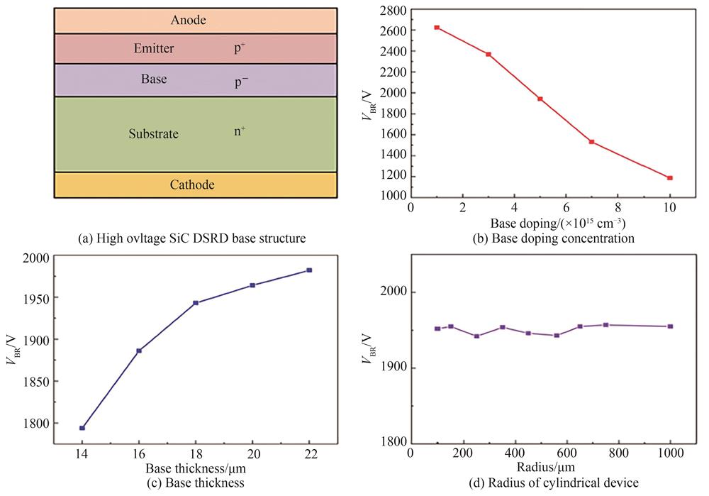
    Fig. 1. Influence of base region on breakdown characteristics of high voltage SiC DSRD devices
    Influence of base region on dynamic characteristics of high voltage SiC DSRD Devices
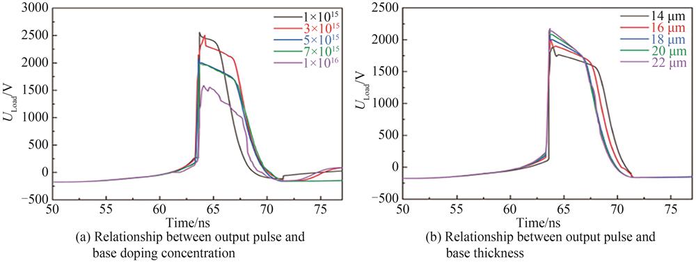
    Fig. 2. Influence of base region on dynamic characteristics of high voltage SiC DSRD Devices
    Schematic of the structure of a high-voltage SiC DSRD device
    Fig. 3. Schematic of the structure of a high-voltage SiC DSRD device
    Simulation of breakdown characteristics of high-voltage SiC DSRD devices
    Fig. 4. Simulation of breakdown characteristics of high-voltage SiC DSRD devices
    High voltage SiC DSRD equivalent model
    Fig. 5. High voltage SiC DSRD equivalent model
    High voltage DSRD pulse source simulation circuit
    Fig. 6. High voltage DSRD pulse source simulation circuit
    The influence of different MOS transistor driving time on the load output pulse
    Fig. 7. The influence of different MOS transistor driving time on the load output pulse
    The effect of the capacitance value of capacitor C1 on the circuit
    Fig. 8. The effect of the capacitance value of capacitor C1 on the circuit
    Influence of DC voltage source V1 on output pulse(V2=60 V)
    Fig. 9. Influence of DC voltage source V1 on output pulse(V2=60 V)
    Output characteristics of pulse source circuit based on high voltage SiC DSRD model
    Fig. 10. Output characteristics of pulse source circuit based on high voltage SiC DSRD model
    Jinlei LI, Jingnan LIU, Jingwen ZHANG, Xin LIU, Shuochen MA, Xun HOU. Structural Design and Pulse Circuit Optimization of High Voltage SiC-based DSRD Devices[J]. Acta Photonica Sinica, 2022, 51(10): 1025001
    Download Citation