• Acta Photonica Sinica
  • Vol. 51, Issue 10, 1025001 (2022)
Jinlei LI1、2、*, Jingnan LIU1、2, Jingwen ZHANG1、2, Xin LIU1、2, Shuochen MA1、2, and Xun HOU1、2
Author Affiliations
  • 1Key Laboratory of Physical Electronics and Devices,Shaanxi Key Lab of Information Photonic Technique,School of Electronic Science and Engineering,Xi'an Jiaotong University,Xi'an 710049
  • 2Institute of Wide Bandgap Semiconductors,Xi'an Jiaotong University,Xi'an 710049
  • show less
    DOI: 10.3788/gzxb20225110.1025001 Cite this Article
    Jinlei LI, Jingnan LIU, Jingwen ZHANG, Xin LIU, Shuochen MA, Xun HOU. Structural Design and Pulse Circuit Optimization of High Voltage SiC-based DSRD Devices[J]. Acta Photonica Sinica, 2022, 51(10): 1025001 Copy Citation Text show less

    Abstract

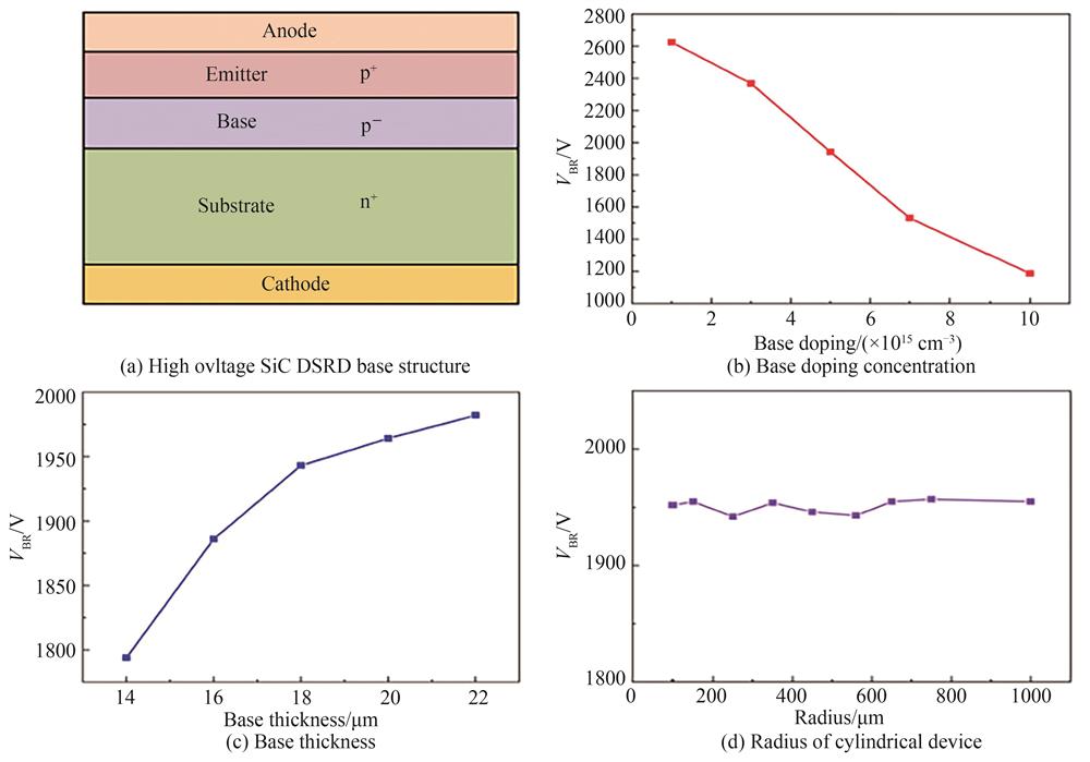
    Ultra-fast High-power Pulse Technology (UHPT) is a technology that converts or releases electromagnetic energy to specific loads in nanoseconds or even sub-nanoseconds to form ultra-high-power pulses. When the input energy is constant, the shorter the output time compression, the higher the pulse power obtained. It has a very broad application in biomedical, food processing, air purification, material modification, high-power microwave, ultra-broad spectrum and other fields.Common techniques that can be used to generate high-power pulses include: 1) (Spark-gap, SG); 2) (Nonlinear Transmission Lines, NLTLs); 3) (Magnetic Pulse Compressor System, MPC); 4) (Semiconductor Solid State Switch) Wait. Although high-voltage SG can achieve high-power nanosecond or even sub-nanosecond pulses, it is limited by factors such as short lifetime, low repetition frequency, and high jitter, and short lifetime will bring high cost consumption in practical applications.Compared with Si materials, wide bandgap semiconductor SiC has a wide bandgap, high thermal conductivity, and relatively mature wafer technology, which makes it very important in high temperature and high power fields. The only group IV-IV compound semiconductor containing Si element has better compatibility with traditional Si process, which can reduce the research and development cycle and cost, and lay a solid foundation for the industrial application of the device. The research on DSRD devices in Russia, Germany and Japan is leading the world. The voltage rise rate of SiC DSRD devices developed by them can reach 2~3 V/ps, which is much higher than that of Si DSRD (0.8~1 V/ps), but has yet to reach its theoretical valuation. However, domestic Si-based DSRD devices can achieve high-voltage pulses of tens of kV, but there are not many researches on SiC-based DSRD devices, which is extremely unfavorable for the realization and application of ultra-fast pulses in China. Therefore, it is necessary to speed up the development and application of SiC DSRD devices. This topic is based on SiC materials to explore the characteristics and processes of DSRD devices.Drift Step Recovery Diode (DSRD) has the advantages of high power, high repetition frequency and low jitter, so it has great potential in the field of ultrafast high power pulse technology. SiC has the characteristics of wide band gap, high thermal conductivity and high critical breakdown field strength, which can meet the commercial applications in high temperature, high frequency and high power fields, and is the best choice for the preparation of new drift step recovery diode materials. Domestic research on SiC drift step recovery diodes is difficult to meet the high-frequency and high-power requirements of ultra-fast high-power pulse switching. In this paper, a SiC DSRD device is designed, its working circuit is optimized, and the SiC reactive ion etching process and n-type ohmic contact process are studied. The main contents are as follows: In order to meet the different application requirements of the device, the corresponding physical model is established, and two SiC DSRD devices are simulated and designed. One is a high-voltage SiC DSRD with a base doping concentration of 5×1015 cm-3 and a thickness of 18μm, a single-chip withstand voltage of over 1 800 V and a switching time of about 500 ps; the other is a low-voltage SiC DSRD with a base thickness of 0.5 μm, a doping concentration of 1×1016 cm-3, and a single-chip withstand voltage of over 53 V. The research on high-voltage SiC DSRD finds that its forward conduction current is negatively correlated with the change of device operating temperature; the low-voltage SiC DSRD device have the largest forward conduction current at 400 K. At the same time, based on the equivalent models of SiC DSRD devices with different withstand voltages, the circuit parameters are optimized, and the high-voltage (2.2 kV) pulse of 8.8 kW and the switching time of about 500 ps and the ultra-fast pulse of 0.11 kW and the switching time of about 60 ps are respectively realized at the load side.
    Jinlei LI, Jingnan LIU, Jingwen ZHANG, Xin LIU, Shuochen MA, Xun HOU. Structural Design and Pulse Circuit Optimization of High Voltage SiC-based DSRD Devices[J]. Acta Photonica Sinica, 2022, 51(10): 1025001
    Download Citation