• Acta Photonica Sinica
  • Vol. 51, Issue 5, 0523001 (2022)
Wenjing XU1、2, Jie CHEN1、*, Zhangqu KUANG3, Li ZHOU1, Ming CHEN1, and Chengbin ZHANG1
Author Affiliations
  • 1Institute of Microelectronics of the Chinese Academy of Sciences,Beijing 100029,China
  • 2University of Chinese Academy of Sciences,Beijing 100049,China
  • 3Will Semiconductor Co. Ltd.,Shanghai 201210,China
  • show less
    DOI: 10.3788/gzxb20225105.0523001 Cite this Article
    Wenjing XU, Jie CHEN, Zhangqu KUANG, Li ZHOU, Ming CHEN, Chengbin ZHANG. Design and Experiment of Low-voltage 4T-PPD Active Pixel[J]. Acta Photonica Sinica, 2022, 51(5): 0523001 Copy Citation Text show less

    Abstract

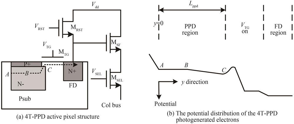
    The 4T Pinned Photodiode (4T-PPD) active pixel is the most widely used pixel structure for CMOS Image Sensor (CIS). In recent years, as the application of CIS has gradually expanded to the Internet of Things (IoT) and Artificial Intelligence (AI) fields, there is an increasing demand for low energy consumption. The basic theory and commonly adopted approach to reduce power consumption are to lower the power supply voltage, while the supply voltage of 4T-PPD is traditionally greater than 2.8 V. In 2016, the study published in JSSC suggested that by improving the timing, the 4T-PPD active pixels could work at 0.9 V, but the readout noise was as high as 83e-rms and the dynamic range was only 50 dB, which could only meet low-quality imaging.Several studies have been conducted on the charge transfer characteristics of traditional high-voltage 4T-PPD. In 2003, FOSSUM E R simulated the charge transfer from PPD to Floating Diffusion (FD) node based on thermionic emission theory. Based on this work, in 2016, HAN Liqiang et al. included non-ideal factors such as the reverse charge injection from FD to PPD. Additionally, in 2019, CAPOCCIA R et al. added an estimate of the thermionic emission barrier height based on the findings of the aforementioned studies. However, these theories were not fully applicable to low-voltage 4T-PPD, since they all assumed a complete photo-generated charge transfer inside the PPD. When the voltage drops, the electrons far away from the transfer gate lack a lateral electric field and stay in the photosensitive area, causing image lag, which will seriously affect the imaging quality.In this paper, a low-voltage 4T-PPD active pixel was designed. First, a theoretical analysis of the internal charge transfer mechanism of PPD was proposed. Three charge transfer mechanisms operate inside the PPD, namely thermal diffusion, self-induced drift, and fringe-field drift. As the charge transfer by fringe-field drift is much faster than thermal diffusion or self-induced drift, the charge transfer time inside the PPD depends predominantly on the distance where the fringing field is absent. According to the derived equations, when the photogenerated charge to the full-well chargeis less than 4%, thermal diffusion is the main mechanism for the no-fringing-field section, and the length of the no-fringing-field section is almost the same. When the photogenerated charge to the full-well chargeis larger than 4%, self-induced drift is the main mechanism for the no-fringing-field section. Moreover, when the transfer gate voltage increases, the length of the no-fringing-field section becomes shorter. As the PPD size decreases, the length of the no-fringing-field section becomes shorter significantly.When the transfer gate voltage drops, the electrons far from the transfer gate lack fringing field and could not be pulled out of the PPD within transfer time, thus resulting in image lag. To solve image lag caused by low-voltage 4T-PPD, and easily achieve it without changing the process steps and conditions, the shape of the PPD layer might be changed. In previous studies, triangle, W-shape, trapezoid, and L-shape PPD have been reported, but all these designs aim at large-sized pixels. For small-sized pixels, the PPD layer should not be cut too much, otherwise, it would affect the full-well capacity and reduce the dynamic range. Therefore, a five-finger pixel layer was proposed to replace the traditional square pixel layer. Compared with conventional rectangular PPD, the five-finger shaped PPD not only reduces the length of the no-fringing-field section but also creates an extra electrical field in the direction of the charge transfer by the narrow width effect. This causes more electrons to be pulled out of the PPD. The proposed five-finger shaped PPD not only can accelerate the electrons transfer from PPD to TG but also meets the requirements of full-well capacity and dynamic range due to the small cut-off area.A prototype sensor was fabricated using a 0.11 µm 1P3M CMOS process. The experiment results show that the residual charge of the designed five-finger 4T-PPD is reduced by 80% compared with the traditional rectangle pixel. The performance of the designed five-finger 4T-PPD with 1.5 V voltage supply is as follows, the full well capacity is 4 928e-, the dynamic range is 67.3 dB, and the random noise is only 1.55e-rms, which are comparable to traditional high-voltage 4T-PPD. The findings presented in this paper provide important guidance for the design of low-voltage 4T-PPD.
    Wenjing XU, Jie CHEN, Zhangqu KUANG, Li ZHOU, Ming CHEN, Chengbin ZHANG. Design and Experiment of Low-voltage 4T-PPD Active Pixel[J]. Acta Photonica Sinica, 2022, 51(5): 0523001
    Download Citation