• Chinese Optics Letters
  • Vol. 20, Issue 1, 013301 (2022)
Jing Yan1、2、*, Xiangwen Fan1, Yifan Liu3, Ying Yu1、2, Yuming Fang1、2, and Ruo-Zhou Li1、2、**
Author Affiliations
  • 1College of Electronic and Optical Engineering & College of Microelectronics, Nanjing University of Posts and Telecommunications, Nanjing 210023, China
  • 2National and Local Joint Engineering Laboratory of RF Integration and Micro-Assembly Technology, Nanjing University of Posts and Telecommunications, Nanjing 210023, China
  • 3Touch and Display Module Development Group, Microsoft Inc., Suzhou 215123, China
  • show less
    DOI: 10.3788/COL202220.013301 Cite this Article Set citation alerts
    Jing Yan, Xiangwen Fan, Yifan Liu, Ying Yu, Yuming Fang, Ruo-Zhou Li. Passive patterned polymer dispersed liquid crystal transparent display[J]. Chinese Optics Letters, 2022, 20(1): 013301 Copy Citation Text show less
    Fabrication process of the patterned PDLC transparent display. (a) Injecting the PDLC precursor. (b) UV exposure. (c) Peeling off the mask.
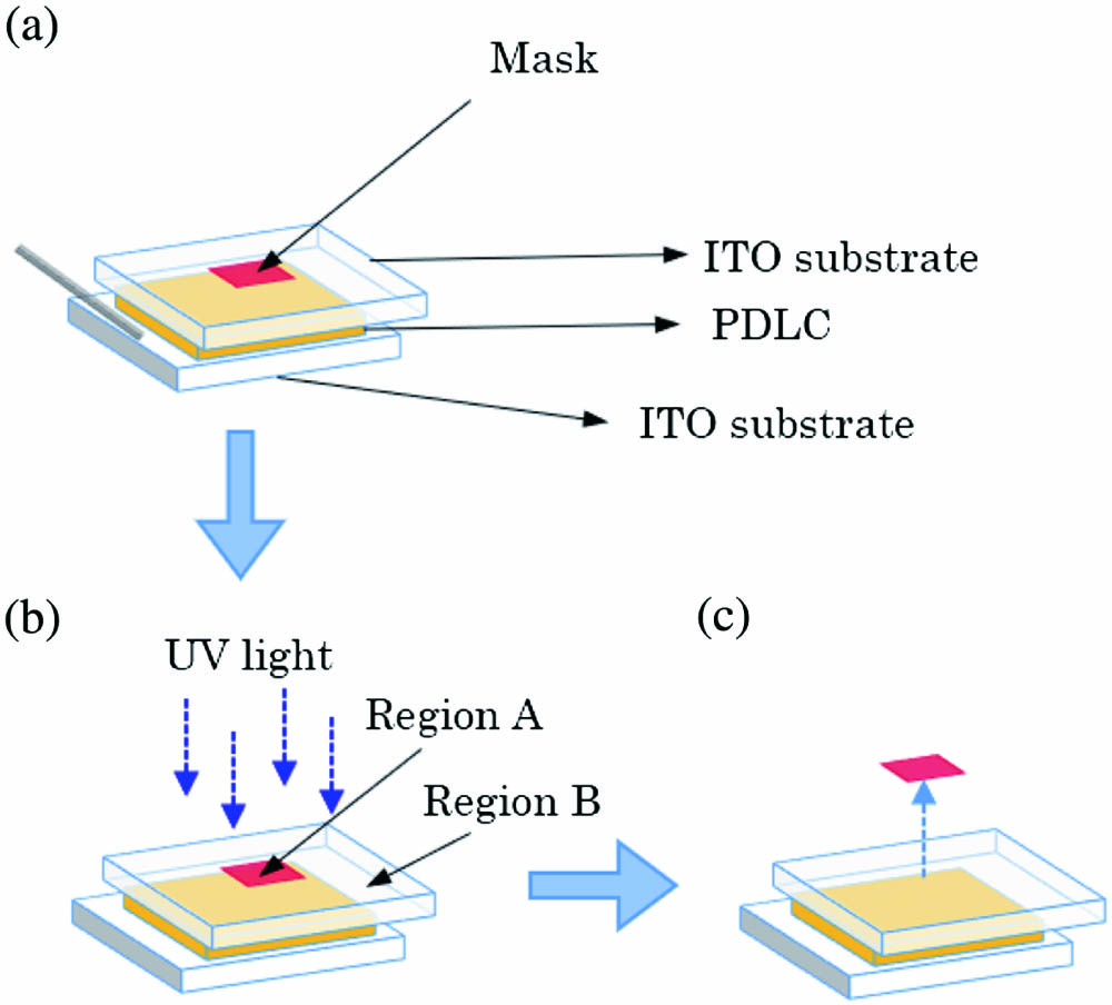
    Fig. 1. Fabrication process of the patterned PDLC transparent display. (a) Injecting the PDLC precursor. (b) UV exposure. (c) Peeling off the mask.
    Working principle of the patterned PDLC transparent display. (a) Voltage-off state. (b) Voltage-on state with V1. (c) Voltage-on state with V2 and V2 > V1.
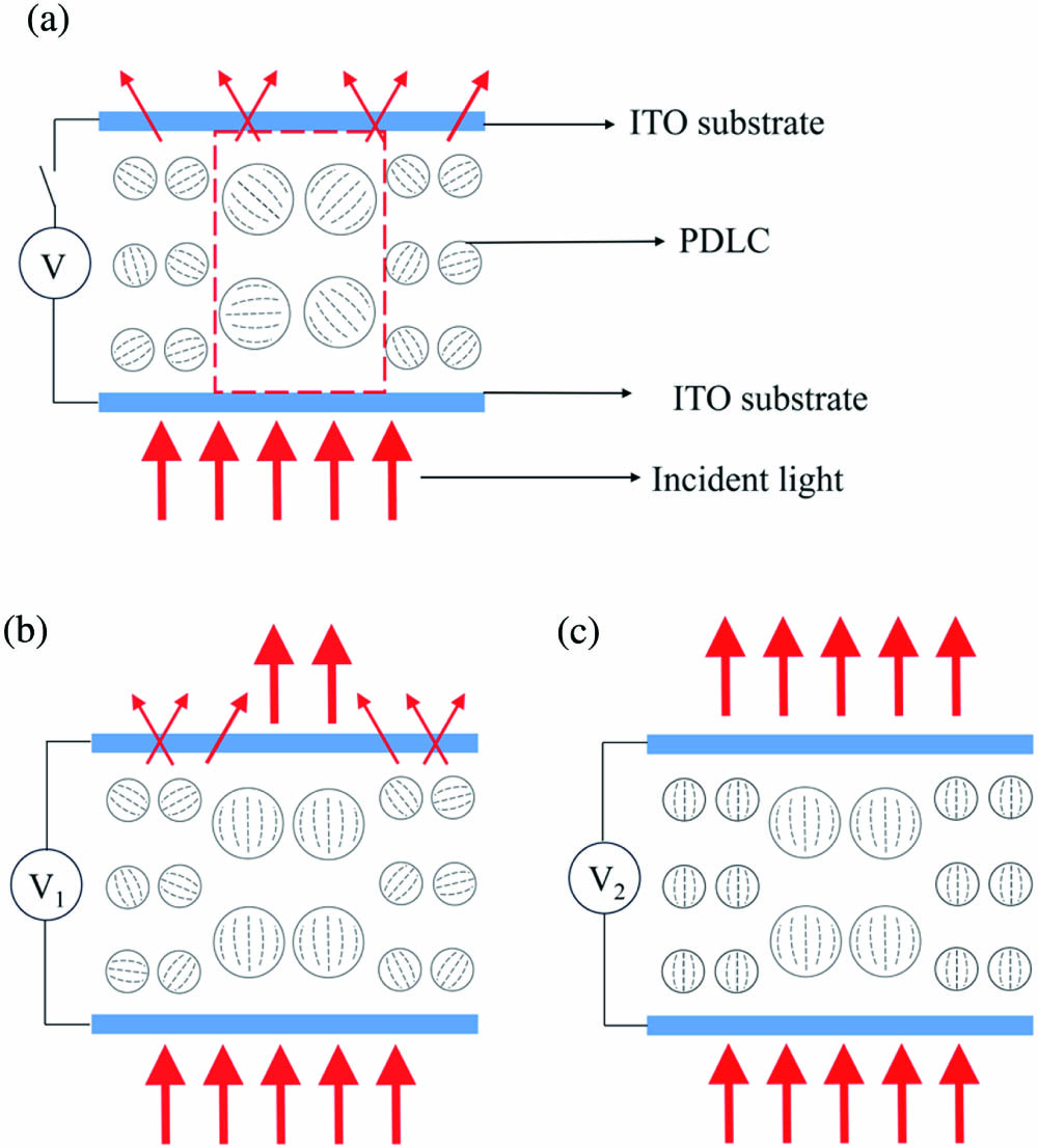
    Fig. 2. Working principle of the patterned PDLC transparent display. (a) Voltage-off state. (b) Voltage-on state with V1. (c) Voltage-on state with V2 and V2 > V1.
    (a) Measured V-T curves of region A and region B of the device. (b) The variation of the transmittance ratio of region A and region B with applied voltage. Insets: the morphologies of the two regions with different applied voltages under a microscope. (I) 0Vrms; (II) 17.6Vrms; (III) 40Vrms.
    Fig. 3. (a) Measured V-T curves of region A and region B of the device. (b) The variation of the transmittance ratio of region A and region B with applied voltage. Insets: the morphologies of the two regions with different applied voltages under a microscope. (I) 0Vrms; (II) 17.6Vrms; (III) 40Vrms.
    SEM images of (a) region A and (b) region B. The droplet size distributions of (c) region A and (d) region B.
    Fig. 4. SEM images of (a) region A and (b) region B. The droplet size distributions of (c) region A and (d) region B.
    Patterned PDLC transparent display is used in shutter mode as smart windows. (a) The display performance for the scenery in the distance. (b) The display performance for the graph nearby.
    Fig. 5. Patterned PDLC transparent display is used in shutter mode as smart windows. (a) The display performance for the scenery in the distance. (b) The display performance for the graph nearby.
    Patterned PDLC transparent display is used in projected display mode. (a) A black card printed with a color pattern behind the device. (b) A phone screen displaying letters behind the device.
    Fig. 6. Patterned PDLC transparent display is used in projected display mode. (a) A black card printed with a color pattern behind the device. (b) A phone screen displaying letters behind the device.
    Response time of region A and region B for the operating voltage of 40Vrms.
    Fig. 7. Response time of region A and region B for the operating voltage of 40Vrms.
    Jing Yan, Xiangwen Fan, Yifan Liu, Ying Yu, Yuming Fang, Ruo-Zhou Li. Passive patterned polymer dispersed liquid crystal transparent display[J]. Chinese Optics Letters, 2022, 20(1): 013301
    Download Citation