
Jing Yan, Xiangwen Fan, Yifan Liu, Ying Yu, Yuming Fang, Ruo-Zhou Li, "Passive patterned polymer dispersed liquid crystal transparent display," Chin. Opt. Lett. 20, 013301 (2022)
- Chinese Optics Letters
- Vol. 20, Issue 1, 013301 (2022)
Abstract
1. Introduction
Transparent displays are favored as next-generation display devices with the characteristics of rendering images on the panel, and the observers can see the scenery from both sides at the same time[
In this Letter, we propose a patterned PDLC transparent display using one-time UV exposure. The device is fabricated by exposing the cell with a uniform UV light through a patterned mask, which selectively attenuates the UV light. The patterned UV light causes patterned polymer concentration of the PDLC, resulting in different voltage-transmittance responses of the device for different regions. Thus, three different states of total scattering, patterned transparent, and total transparent can be realized by applying proper driving voltages, respectively.
2. Fabrication and Working Principle
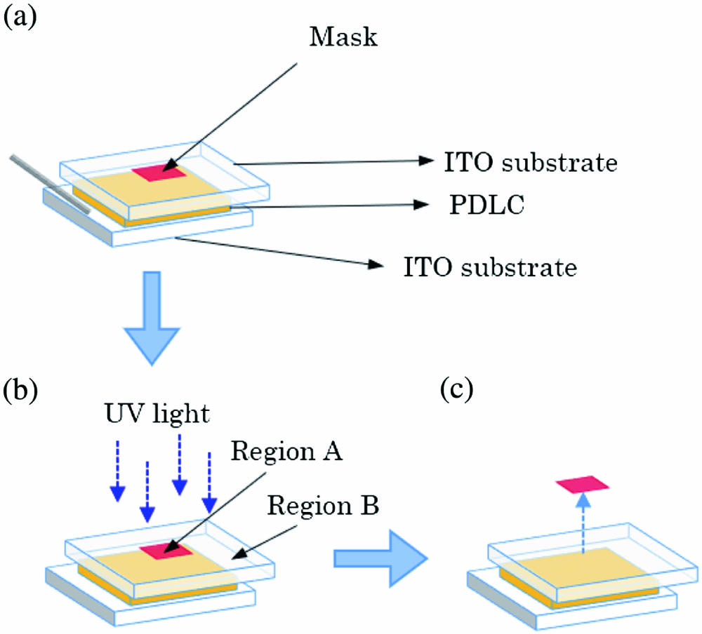
Figure 1 illustrates the fabrication process of a patterned PDLC transparent display. The PDLC employed in this Letter is a mixture composed of 60% (mass fraction) liquid crystal E7 (HCCH) and 40% (mass fraction) monomer NOA65 (Norland). The precursor in the isotropic state (
Sign up for Chinese Optics Letters TOC. Get the latest issue of Chinese Optics Letters delivered right to you!Sign up now
![]()
Figure 1.Fabrication process of the patterned PDLC transparent display. (a) Injecting the PDLC precursor. (b) UV exposure. (c) Peeling off the mask.
The electro-optical property of PDLC film is determined by the PDLC droplet size. Higher UV intensity results in smaller droplets and higher threshold voltage, while lower UV intensity leads to larger droplets and lower threshold voltage[
![]()
Figure 2.Working principle of the patterned PDLC transparent display. (a) Voltage-off state. (b) Voltage-on state with V1. (c) Voltage-on state with V2 and V2 > V1.
3. Results and Discussions
To investigate the electro-optical properties of the two regions, we measure the voltage-transmittance curves (V-T curves) of region A and region B. The device is driven by a square-wave voltage signal of 1 kHz in frequency, and the transmitted light intensity through the device is received by a photodetector (New Focus 2031) and recorded by an oscilloscope (Tektronix TBS1102X). The blue square dotted line represents the measured V-T curve of the PDLC in region A, while the red circle dotted line indicates the measured data for region B in Fig. 3(a). It is clearly shown that the cured PDLC in region A has a lower threshold voltage of
![]()
Figure 3.(a) Measured V-T curves of region A and region B of the device. (b) The variation of the transmittance ratio of region A and region B with applied voltage. Insets: the morphologies of the two regions with different applied voltages under a microscope. (I) 0Vrms; (II) 17.6Vrms; (III) 40Vrms.
The transmittance ratio of region A and region B (
![]()
Figure 4.SEM images of (a) region A and (b) region B. The droplet size distributions of (c) region A and (d) region B.
Figure 5 demonstrates that the patterned PDLC transparent display can be used in shutter mode as a smart window. The photographs of the total scattering, patterned transparent, and total transparent modes of the device for the scenery far away and the graph nearby are shown in Figs. 5(a) and 5(b), respectively. At the voltage-off state, neither the scenery nor the graph can be seen through the device, due to the strong scattering of the device. As a
![]()
Figure 5.Patterned PDLC transparent display is used in shutter mode as smart windows. (a) The display performance for the scenery in the distance. (b) The display performance for the graph nearby.
As the proposed device can operate in the scattering state or transparent state by controlling the applied voltage, the device working in partial scattering mode or total scattering mode can also be used as a specific screen for the projected image. Figure 6 demonstrates the performance of the patterned transparent display in the projected display mode. A projector (LG PB63U) projects an image containing colorful geometric patterns and letters on the device and places a black card printed with a color pattern or a phone screen displayed with letters behind it. Although the projected image is more or less scattered, the image information can be still distinguished at the voltage-off state. The information behind the device cannot be seen in this case. Then, when a voltage of
![]()
Figure 6.Patterned PDLC transparent display is used in projected display mode. (a) A black card printed with a color pattern behind the device. (b) A phone screen displaying letters behind the device.
The response time of the proposed device is also measured for the different regions, as shown in Fig. 7. The blue triangle line and red square dashed line represent the transmittance of region A and region B, and the black line stands for the operating voltage of
![]()
Figure 7.Response time of region A and region B for the operating voltage of 40Vrms.
4. Conclusion
In conclusion, a patterned PDLC transparent display using one-time UV exposure is proposed. The patterned intensity distribution of UV light is achieved by exposing the device through an attached mask with a selective attenuation pattern, leading to the patterned polymer concentration of the PDLC. The voltage-transmittance response of the device for region A and region B is quite different in turn. Thus, three different states of total scattering, patterned transparent, and total transparent can be realized. The patterned PDLC transparent display used in shutter mode as smart windows and in projected display mode is demonstrated. This patterned PDLC transparent display can be optimized for smart windows with customized patterns or logos and potential applications in the field of projected transparent displays.
References
[1] C.-W. Su, M.-Y. Chen. Polymer-dispersed liquid crystal applied in active-matrix transparent display. J. Disp. Technol., 10, 683(2014).
[2] C.-W. Chen, A. N. Brigeman, T.-J. Ho, I. C. Khoo. Normally transparent smart window based on electrically induced instability in dielectrically negative cholesteric liquid crystal. Opt. Mater. Express., 8, 691(2018).
[3] H. Peng, D. Cheng, J. Han, C. Xu, W. Song, L. Ha, J. Yang, Q. Hu, Y. Wang. Design and fabrication of a holographic head-up display with asymmetric field of view. Appl. Opt., 53, H177(2014).
[4] K. Akşit, W. Lopes, J. Kim, P. Shirley, D. Luebke. Near-eye varifocal augmented reality display using see-through screens. ACM Trans. Graphic., 36, 1(2017).
[5] Z. Chen, X. Sang, H. Li, Y. Wang, L. Zhao. Ultra-lightweight and wide field of view augmented reality virtual retina display based on optical fiber projector and volume holographic lens. Chin. Opt. Lett., 17, 090901(2019).
[6] S. Ikawa, N. Takada, H. Araki, H. Arali, H. Niwase, H. Sannomiya, H. Nakayama, M. Oikawa, Y. Mori, T. Kakue, T. Shimobaba, T. Ito. Real-time color holographic video reconstruction using multiple-graphics processing unit cluster acceleration and three spatial light modulators. Chin. Opt. Lett., 18, 010901(2020).
[7] J. Chung, J. Lee, J. Choi, C. Park, J. Ha, H. Chung, S. S. Kim. Transparent AMOLED display based on bottom emission structure. SID Symposium Digest of Technical Papers, 148(2010).
[8] M. S. Chan Il Park, M. A. Kim, D. Kim, H. Jung, M. Cho, S. H. Lee, H. Lee, S. Min, J. Kim, M. Kim, J.-H. Park, S. Kwon, B. Kim, S. J. Kim, W. Park, J.-Y. Yang, S. Yoon, I. Kang. World 1st large size 77-inch transparent flexible OLED display. SID Symposium Digest of Technical Papers, 710(2018).
[9] C.-W. Su, C.-C. Liao, M.-Y. Chen. Color transparent display using polymer-dispersed liquid crystal. J. Disp. Technol., 12, 31(2016).
[10] J. W. Kim, J. M. Myoung. Flexible and transparent electrochromic displays with simultaneously implementable subpixelated ion gel-based viologens by multiple patterning. Adv. Funct. Mater., 29, 1908911(2019).
[11] C. W. Hsu, B. Zhen, W. Qiu, O. Shapira, B. G. DeLacy, J. D. Joannopoulos, M. Soljacic. Transparent displays enabled by resonant nanoparticle scattering. Nat. Commun., 5, 3152(2014).
[12] Z. He, K. Yin, S. T. Wu. Passive polymer-dispersed liquid crystal enabled multi-focal plane displays. Opt. Express, 28, 15294(2020).
[13] M. Xu, H. Hua. Geometrical-lightguide-based head-mounted lightfield displays using polymer-dispersed liquid-crystal films. Opt. Express, 28, 21165(2020).
[14] I. Abdulhalim, P. L. Madhuri, M. Diab, T. Mokari. Novel easy to fabricate liquid crystal composite with potential for electrically or thermally controlled transparency windows. Opt. Express, 27, 17387(2019).
[15] V. Sharma, P. Kumar, A. Sharma, C. Jaggi, K. K. Raina. Droplet configuration control with orange azo dichroic dye in polymer dispersed liquid crystal for advanced electro-optic characteristics. J. Mol. Liq., 233, 122(2017).
[16] P. Kumar, V. Sharma, C. Jaggi, K. K. Raina. Dye-dependent studies on droplet pattern and electro-optic behaviour of polymer dispersed liquid crystal. Liquid Cryst., 44, 757(2017).
[17] P. Kumar, V. Sharma, C. Jaggi, P. Malik, K. K. Raina. Orientational control of liquid crystal molecules via carbon nanotubes and dichroic dye in polymer dispersed liquid crystal. Liquid Cryst., 44, 843(2017).
[18] L. De Sio, E. Ouskova, P. Lloyd, R. Vergara, N. Tabiryan, T. J. Bunning. Light-addressable liquid crystal polymer dispersed liquid crystal. Opt. Mater. Express, 7, 1581(2017).
[19] M. H. Saeed, S. Zhang, M. Yu, L. Zhou, J. Huang, Q. Feng, H. Lin, X. Wang, J. Hu, L. Zhang, H. Yang. Effects of oxygen heterocyclic acrylate monomers on the morphologies and electro-optical properties of polymer dispersed liquid crystal composite films. Optik, 229, 166254(2021).
[20] H. Jiang, W. Cai, K. Li, M. Cheng, V. Kumar, Z. Yin, D. Gérard, D. Luo, Q. Mu, Y. Liu. Holographically fabricated, highly reflective nanoporous polymeric distributed Bragg reflectors with red, green, and blue colors. Chin. Opt. Lett., 18, 080007(2020).
[21] Z. Diao, L. Kong, J. Yan, J. Guo, X. Liu, L. Xuan, L. Yu. Electrically tunable holographic waveguide display based on holographic polymer dispersed liquid crystal grating. Chin. Opt. Lett., 17, 012301(2019).
[22] D.-J. Kim, D. Y. Hwang, J.-Y. Park, H.-K. Kim. Liquid crystal-based flexible smart windows on roll-to-roll slot die-coated Ag nanowire network films. J. Alloy. Compd., 765, 1090(2018).
[23] S.-L. Hou, W.-K. Choi, G.-D. Su. High efficient polymer dispersed liquid crystal for ultra-bright projected image. Proc. SPIE, 8828, 882816(2013).
[24] H. L. Zhang, H. Deng, J. J. Li, M. Y. He, D. H. Li, Q. H. Wang. Integral imaging-based 2D/3D convertible display system by using holographic optical element and polymer dispersed liquid crystal. Opt. Lett., 44, 387(2019).
[25] F. Ahmad, M. Jamil, J. W. Lee, S. R. Kim, Y. J. Jeon. The effect of UV intensities and curing time on polymer dispersed liquid crystal (PDLC) display: a detailed analysis study. Electron. Mater. Lett., 12, 685(2016).
[26] Y. Liu, S. Xu, D. Xu, J. Yan, Y. Gao, S.-T. Wu. A hysteresis-free polymer-stabilised blue-phase liquid crystal. Liquid Cryst., 41, 1339(2014).
[27] D. K. Yang, S. T. Wu. Fundamentals of Liquid Crystal Devices(2014).


Set citation alerts for the article
Please enter your email address

© Copyright 2018-2021 | Chinese Laser Press. All Rights Reserved 沪ICP备15018463号-20