
Huabin Yu, Zhongjie Ren, Muhammad Hunain Memon, Shi Fang, Danhao Wang, Zhongling Liu, Haochen Zhang, Feng Wu, Jiangnan Dai, Changqing Chen, Haiding Sun, "Cascaded deep ultraviolet light-emitting diode via tunnel junction," Chin. Opt. Lett. 19, 082503 (2021)
- Chinese Optics Letters
- Vol. 19, Issue 8, 082503 (2021)
Abstract
1. Introduction
Deep ultraviolet (DUV) light has various applications in the areas of air/water purification, disinfection, sterilization, and free-space optical communication[
Recently, the implementation of the tunnel junction (TJ) structure has gained remarkable attention in the development of high-efficiency group-III-nitride-based LEDs. In one aspect, the high-resistance
2. Device Architecture
In this study, three devices are constructed and investigated. Firstly, a conventional DUV LED (C-DUV LED) emitting at 284.5 nm, experimentally reported by Yan et al.[
Sign up for Chinese Optics Letters TOC. Get the latest issue of Chinese Optics Letters delivered right to you!Sign up now
![]()
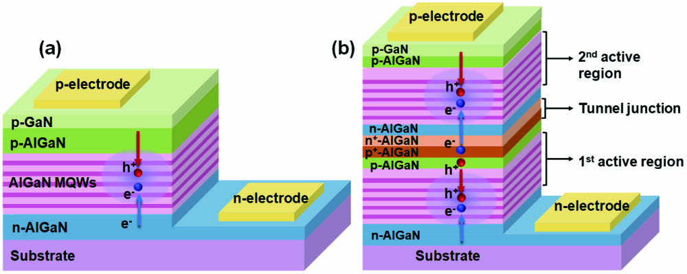
Figure 1.(a) Schematics of the C-DUV LED and (b) the TJC-DUV LED.
The simulator is provided by Crosslight Inc. APSYS (version 2018), which is widely used in the investigation of the III-nitride-based LEDs in both academia and industry[
3. Results and Discussion
The optical performance of the investigated three DUV LEDs is exhibited in Figs. 2(a)–2(d). We found that the simulated results [blue curves in Figs. 2(a) and 2(d)] perfectly matched with those experimental results extracted from the reference LED (orange squares from Yan et al.[
![]()
Figure 2.(a) LOPs as functions of the injection currents for the C-DUV LEDs with five QWs, 10 QWs, and the TJC-DUV LED, respectively. (b) The EL spectra of the three DUV LEDs. (c) The LOPs and IQEs as functions of the number of the QWs in the C-DUV LED at 60 mA. (d) The current-voltage characteristics of the three investigated samples.
There is one question to be answered: can we simply increase the number of QWs to boost the optical performance instead of using a complex TJC structure? In other words, it might not be necessary to build a TJC structure to enhance the performance of the DUV LED device. To address this issue, we investigated the LOP and IQE performance of a C-DUV LED by increasing its number of QWs from 1 to 10. The results are shown in Fig. 2(c). When the QW number increased from 1 to 4, the LOP and IQE of the C-DUV LED can be enhanced dramatically, attributed to the decreased electron current overflow[
The output power of the TJC-DUV LED is much larger than that of the C-DUV LED with the same power supply, as compared in Fig. 3(a). The WPEs for C-DUV LEDs and a TJC-DUV LED are demonstrated in Fig. 3(b). The C-DUV LED with 10 QWs exhibits a lowered WPE than that with five QWs due to the trade-off between the number of QWs and carrier concentration in the active region. In comparison, the WPE of the TJC-DUV LED is significantly increased, resulting from the reduced injection current level at the same value of LOP among the three devices. It can be noted that the WPE of the TJC-DUV LED is a little smaller at a low current level, but it has a much larger value at a high current level than that of the C-DUV LED with five QWs. To be more specific, the WPE of the TJC-DUV LED is significantly boosted by 25% at 60 mA than that of the C-DUV LED with five QWs. It is mainly attributed to the increasing operation bias of the TJC-DUV LED compared with the bias of the C-DUV LED with five QWs.
![]()
Figure 3.(a) Required input power of the C-DUV LEDs with five QWs, 10 QWs, and TJC-DUV LED, respectively, as a function of output power. (b) The corresponding WPE values of the three devices as functions of current.
Figure 4 represents the band diagrams of the TJC-DUV LED. In the C-DUV LED, the recombination of the electrons and holes takes place only once within the active region to generate photons. In contrast, the photon generation process can occur in both active regions in the TJC-DUV LED, enabling a dual radiative recombination process, as illustrated in Fig. 4. A mode of smooth carrier transport and injection can be provided by the TJ structure, which bridged the two active regions. Specifically, the electrons in the
![]()
Figure 4.Energy band diagram for the TJC-DUV LED at 60 mA.
The e–h concentrations and radiative recombination rate profiles in the active regions are further investigated to explore the underlying mechanism of the performance enhancement for the TJC-DUV LED. As illustrated in Figs. 5(a1) and 5(b1), the e–h concentration in each QW is drastically reduced when the number of QWs is increased from 5 to 10 in the C-DUV LED. Consequently, the C-DUV LED with 10 QWs exhibits lower radiative recombination rates within the active region in comparison with the C-DUV LED with five QWs, as exhibited in Figs. 5(a2) and 5(b2). On the contrary, the e–h concentration within the two active regions (10 QWs in total) in the TJC-DUV LED remains at the same level as those in the C-DUV LED with five QWs, according to Figs. 5(a1) and 5(c1). The enhanced e–h concentration within the two active regions of the TJC-DUV LED can be ascribed to the dual injection of the electrons and holes in two PIN junctions connected via a TJC structure. Besides, the multiple radiative recombination behavior is also observed in both two active regions, as illustrated in Fig. 5(c2). As shown in Figs. 5(d) and 5(e), the non-radiative recombination rates of the TJC-DUV LED are obviously lower in each QW than that of the C-DUV LED. Hence, with the same radiative rates, the TJC-DUV LEDs possess a significantly higher IQE, as presented in Fig. 5(f), which is attributed to the LOP enhancement of the TJC-DUV LED rather than that of the single C-DUV LED by more than 100%.
![]()
Figure 5.e–h concentrations within active regions for (a1) the C-DUV LED with five QWs, (b1) the C-DUV LED with 10 QWs, and (c1) the TJC-DUV LED, respectively. The radiative recombination rates within the active regions for (a2) the C-DUV LED with five QWs, (b2) the C-DUV LED with 10 QWs, and (c2) the TJC-DUV LED. The non-radiative recombination rates within the active regions at 60 mA for (d) the C-DUV LED and (e) the TJC-DUV LED. (f) The IQE values of the two devices as functions of current.
4. Conclusion
In summary, we have numerically investigated the unique TJC-DUV LED with cascaded active regions connected by a TJ. The simulation results show that introducing the TJC structure in the DUV LEDs can successfully enable the repeated use of electrons and holes for radiative recombination and consequently produce a significantly enhanced LOP and WPE of the device. The proposed TJC structure provides a reliable and cost-effective method to achieve high-performance DUV LEDs, even possibly in high-power DUV lasers of the future.
References
[1] H. Sun, S. Mitra, R. C. Subedi, Y. Zhang, W. Guo, J. Ye, M. K. Shakfa, T. K. Ng, B. S. Ooi, I. S. Roqan, Z. Zhang, J. Dai, C. Chen, S. Long. Unambiguously enhanced ultraviolet luminescence of AlGaN wavy quantum well structures grown on large misoriented sapphire substrate. Adv. Funct. Mater., 29, 1905445(2019).
[2] X. Huang, F. Yang, J. Song. Hybrid LD and LED-based underwater optical communication: state-of-the-art, opportunities, challenges, and trends. Chin. Opt. Lett., 17, 100002(2019).
[3] P. Tian, H. Chen, P. Wang, X. Liu, X. Chen, G. Zhou, S. Zhang, J. Lu, P. Qiu, Z. Qian, X. Zhou, Z. Fang, L. Zheng, R. Liu, X. Cui. Absorption and scattering effects of Maalox, chlorophyll, and sea salt on a micro-LED-based underwater wireless optical communication. Chin. Opt. Lett., 17, 100010(2019).
[4] N. Lobo-Ploch, F. Mehnke, L. Sulmoni, H. K. Cho, M. Guttmann, J. Glaab, K. Hilbrich, T. Wernicke, S. Einfeldt, M. Kneissl. Milliwatt power 233 nm AlGaN-based deep UV-LEDs on sapphire substrates. Appl. Phys. Lett., 117, 111102(2020).
[5] Z. Ma, A. Almalki, X. Yang, X. Wu, X. Xi, J. Li, S. Lin, X. Li, S. Alotaibi, M. A. Huwayz, M. Henini, L. Zhao. The influence of point defects on AlGaN-based deep ultraviolet LEDs. J. Alloys Compd., 845, 156177(2020).
[6] N. H. Tran, B. H. Le, S. Zhao, Z. Mi. On the mechanism of highly efficient p-type conduction of Mg-doped ultra-wide-bandgap AlN nanostructures. Appl. Phys. Lett., 110, 032102(2017).
[7] Y.-K. Kuo, J.-Y. Chang, H.-T. Chang, F.-M. Chen, Y.-H. Shih, B.-T. Liou. Polarization effect in AlGaN-based deep-ultraviolet light-emitting diodes. IEEE J. Quantum Electron., 53, 3300106(2016).
[8] S. Zhang, S. Wang, J. Zhang, H. Long, Y. Gao, J. Dai, C. Chen. TE/TM mode full-spatial decomposition of AlGaN-based deep ultraviolet light-emitting diodes. J. Phys. D: Appl. Phys., 53, 195102(2020).
[9] Z. Ren, H. Yu, Z. Liu, D. Wang, C. Xing, H. Zhang, C. Huang, S. Long, H. Sun. Band engineering of III-nitride-based deep-ultraviolet light-emitting diodes: a review. J. Phys. D: Appl. Phys., 53, 073002(2019).
[10] Y. Zheng, J. Zhang, L. Chang, C. Chu, K. Tian, Q. Zheng, Q. Li, Y. Zhang, W. Bi, Z.-H. Zhang. Understanding omni-directional reflectors and nominating more dielectric materials for deep ultraviolet light-emitting diodes with inclined sidewalls. J. Appl. Phys., 128, 093106(2020).
[11] J. Yun, H. Hirayama. Investigation of the light-extraction efficiency in 280 nm AlGaN-based light-emitting diodes having a highly transparent p-AlGaN layer. J. Appl. Phys., 121, 013105(2017).
[12] J. W. Lee, G. Ha, J. Park, H. G. Song, J. Y. Park, J. Lee, Y.-H. Cho, J.-L. Lee, J. K. Kim, J. K. Kim. AlGaN deep-ultraviolet light-emitting diodes with localized surface plasmon resonance by a high-density array of 40 nm Al nanoparticles. ACS Appl. Mater. Interfaces, 12, 36339(2020).
[13] T. H. Lee, B. R. Lee, K. R. Son, H. W. Shin, T. G. Kim. Highly efficient deep-UV light-emitting diodes using AlN-based deep-UV-transparent glass electrodes. ACS Appl. Mater. Interfaces, 9, 43774(2017).
[14] C. Huang, H. Zhang, H. Sun. Ultraviolet optoelectronic devices based on AlGaN-SiC platform: towards monolithic photonics integration system. Nano Energy, 77, 105149(2020).
[15] Y. Nagasawa, R. Sugie, K. Kojima, A. Hirano, M. Ippommatsu, Y. Honda, H. Amano, I. Akasaki, S. F. Chichibu. Two-dimensional analysis of the nonuniform quantum yields of multiple quantum wells for AlGaN-based deep-ultraviolet LEDs grown on AlN templates with dense macrosteps using cathodoluminescence spectroscopy. J. Appl. Phys., 126, 215703(2019).
[16] B. So, C. Cheon, J. Lee, J. Lee, T. Kwak, U. Choi, J. Song, J. Chang, O. Nam. Epitaxial growth of deep ultraviolet light emitting diodes with two-step n-AlGaN layer. Thin Solid Films, 708, 138103(2020).
[17] T. Wei, S. M. Islam, U. Jahn, J. Yan, K. Lee, S. Bharadwaj, X. Ji, J. Wang, J. Li, V. Protasenko, H. (Grace) Xing, D. Jena. GaN/AlN quantum-disk nanorod 280 nm deep ultraviolet light emitting diodes by molecular beam epitaxy. Opt. Lett., 45, 121(2020).
[18] A. Pandey, W. Shin, J. Gim, R. Hovden, Z. Mi. High-efficiency AlGaN/GaN/AlGaN tunnel junction ultraviolet light-emitting diodes. Photon. Res., 8, 331(2020).
[19] Y. Zhang, S. Krishnamoorthy, F. Akyol, A. A. Allerman, M. W. Moseley, A. M. Armstrong, S. Rajan. Design and demonstration of ultra-wide bandgap AlGaN tunnel junctions. Appl. Phys. Lett., 109, 121102(2016).
[20] J. Piprek. Origin of InGaN/GaN light-emitting diode efficiency improvements using tunnel-junction-cascaded active regions. Appl. Phys. Lett., 104, 051118(2014).
[21] Y.-K. Kuo, Y.-H. Shih, J.-Y. Chang, F.-M. Chen, M.-L. Lee, J.-K. Sheu. Theoretical investigation of efficient green tunnel-junction light-emitting diodes. IEEE Electron Device Lett., 38, 75(2016).
[22] Y.-H. Shih, J.-Y. Chang, Y.-K. Kuo, F.-M. Chen, M.-F. Huang, M.-L. Lee, J.-K. Sheu. Design of GaN-based multicolor tunnel-junction light-emitting diodes. IEEE Trans. Electron Devices, 65, 165(2017).
[23] S.-J. Chang, W.-H. Lin, C.-T. Yu. GaN-based multi quantum well light-emitting diodes with tunnel-junction-cascaded active regions. IEEE Electron Device Lett., 36, 366(2015).
[24] C. H. Chen, S.-J. Chang, Y.-K. Su, J. K. Sheu, J. F. Chen, C. H. Kuo, Y. C. Lin. Nitride-based cascade near white light-emitting diodes. IEEE Photon. Technol. Lett., 14, 908(2002).
[25] H. Zhao, G. Liu, J. Zhang, J. D. Poplawsky, V. Dierolf, N. Tansu. Approaches for high internal quantum efficiency green InGaN light-emitting diodes with large overlap quantum wells. Opt. Express, 19, A991(2011).
[26] H. Zhao, G. Liu, R. A. Arif, N. Tansu. Current injection efficiency induced efficiency-droop in InGaN quantum well light-emitting diodes. Solid-State Electron., 54, 1119(2010).
[27] J. Yan, J. Wang, Y. Zhang, P. Cong, L. Sun, Y. Tian, C. Zhao, J. Li. AlGaN-based deep-ultraviolet light-emitting diodes grown on high-quality AlN template using MOVPE. J. Crystal Growth, 414, 254(2015).
[28] Y. Zhang, S. Krishnamoorthy, F. Akyol, S. Bajaj, A. A. Allerman, M. W. Moseley, A. M. Armstrong, S. Rajan. Tunnel-injected sub-260 nm ultraviolet light emitting diodes. Appl. Phys. Lett., 110, 201102(2017).
[29] C.-C. Shen, Y.-T. Lu, Y.-W. Yeh, C.-Y. Chen, Y.-T. Chen, C.-W. Sher, P.-T. Lee, Y.-H. Shih, T.-C. Lu, T. Wu, C.-H. Chiu, H.-C. Kuo. Design and fabrication of the reliable GaN based vertical-cavity surface-emitting laser via tunnel junction. Crystals, 9, 187(2019).
[31] J.-Y. Chang, B.-T. Liou, M.-F. Huang, Y.-H. Shih, F.-M. Chen, Y.-K. Kuo. High-efficiency deep-ultraviolet light-emitting diodes with efficient carrier confinement and high light extraction. IEEE Trans. Electron Devices, 66, 976(2019).
[32] H. Yu, Z. Ren, H. Zhang, J. Dai, C. Chen, S. Long, H. Sun. Advantages of AlGaN-based deep-ultraviolet light-emitting diodes with an Al-composition graded quantum barrier. Opt. Express, 27, A1544(2019).
[33] J. L. Moll. Physics of Semiconductors(1964).
[34] M. F. Schubert. Interband tunnel junctions for wurtzite III-nitride semiconductors based on heterointerface polarization charges. Phys. Rev. B, 81, 035303(2010).
[35] S. Tan, J. Zhang, T. Egawa, G. Chen. Influence of quantum-well number and an AlN electron blocking layer on the electroluminescence properties of AlGaN deep ultraviolet light-emitting diodes. Appl. Sci., 8, 2402(2018).


Set citation alerts for the article
Please enter your email address

© Copyright 2018-2021 | Chinese Laser Press. All Rights Reserved 沪ICP备15018463号-20