• Acta Optica Sinica
  • Vol. 40, Issue 8, 0814001 (2020)
Yingying Yan1、2, Zhiwen Chen1、2, Jian Qiu1、2、*, Kefu Liu1、2, and Jianwei Zhang3
Author Affiliations
  • 1Engineering Research Center of Advanced Lighting Technology, Ministry of Education, Fudan University, Shanghai 200433, China
  • 2Department of Light Sources and Illuminating Engineering, School of Information Science and Technology, Fudan University, Shanghai 200433, China
  • 3State Key Laboratory of Luminescence and Applications, Changchun Institute of Optics, Fine Mechanics and Physics, Chinese Academy of Sciences, Changchun, Jilin 130033, China
  • show less
    DOI: 10.3788/AOS202040.0814001 Cite this Article Set citation alerts
    Yingying Yan, Zhiwen Chen, Jian Qiu, Kefu Liu, Jianwei Zhang. Effect of Package on Luminescence Characteristics of High-Power VCSEL with Narrow Pulse[J]. Acta Optica Sinica, 2020, 40(8): 0814001 Copy Citation Text show less
    Cross-sectional diagram of VCSEL array
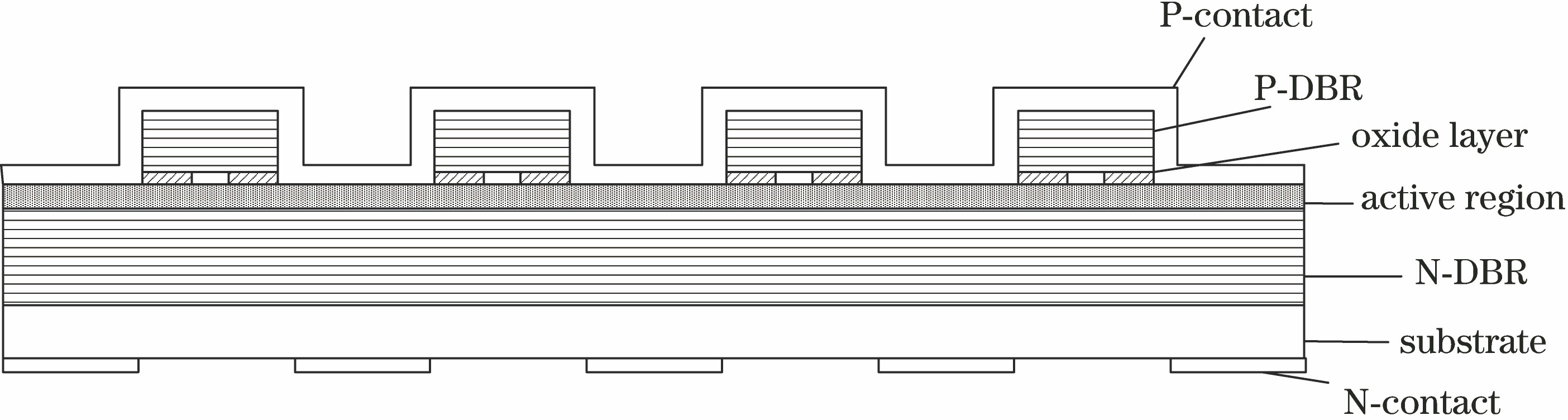
    Fig. 1. Cross-sectional diagram of VCSEL array
    Photograph of VCSEL with bare chip
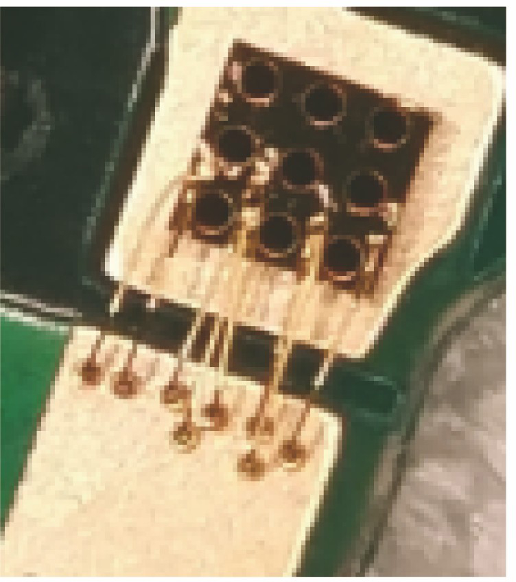
    Fig. 2. Photograph of VCSEL with bare chip
    Photograph of VCSEL with TO package. (a) Side view; (b) top view
    Fig. 3. Photograph of VCSEL with TO package. (a) Side view; (b) top view
    VCSEL with TO package. (a) Diagram of configuration; (b) equivalent circuit
    Fig. 4. VCSEL with TO package. (a) Diagram of configuration; (b) equivalent circuit
    Simplified diagram of drive circuit
    Fig. 5. Simplified diagram of drive circuit
    Simplified diagram of PCB. (a) Top view; (b) bottom view; (c) side view
    Fig. 6. Simplified diagram of PCB. (a) Top view; (b) bottom view; (c) side view
    Voltage and current simulation waveforms at both ends of VCSEL with different Ls (C=10 nF, V=90 V)
    Fig. 7. Voltage and current simulation waveforms at both ends of VCSEL with different Ls (C=10 nF, V=90 V)
    Voltage and current simulation waveforms at both ends of VCSEL with different Rs (C=10 nF, V=90 V)
    Fig. 8. Voltage and current simulation waveforms at both ends of VCSEL with different Rs (C=10 nF, V=90 V)
    Pulse waveforms of voltage and current at both ends of VCSEL (C=10 nF, V=90 V). (a) VCSEL with TO package; (b) VCSEL with bare chip
    Fig. 9. Pulse waveforms of voltage and current at both ends of VCSEL (C=10 nF, V=90 V). (a) VCSEL with TO package; (b) VCSEL with bare chip
    Optical pulse waveforms of VCSEL with TO package and VCSEL with bare chip (C=10 nF, V=90 V)
    Fig. 10. Optical pulse waveforms of VCSEL with TO package and VCSEL with bare chip (C=10 nF, V=90 V)
    Relationship between peak current and peak voltage for VCSEL with TO package and VCSEL with bare chip
    Fig. 11. Relationship between peak current and peak voltage for VCSEL with TO package and VCSEL with bare chip
    Comparison of simulated and experimental waveform. (a) VCSEL with TO package; (b) VCSEL with bare chip
    Fig. 12. Comparison of simulated and experimental waveform. (a) VCSEL with TO package; (b) VCSEL with bare chip
    Relationship between peak power of optical pulse and peak current of VCSEL with TO package and VCSEL with bare chip (C=10 nF, V=30--90 V)
    Fig. 13. Relationship between peak power of optical pulse and peak current of VCSEL with TO package and VCSEL with bare chip (C=10 nF, V=30--90 V)
    Relationship between power conversion efficiency and peak current of VCSEL with TO package and VCSEL with bare chip (C=10 nF, V=30--90 V)
    Fig. 14. Relationship between power conversion efficiency and peak current of VCSEL with TO package and VCSEL with bare chip (C=10 nF, V=30--90 V)
    Yingying Yan, Zhiwen Chen, Jian Qiu, Kefu Liu, Jianwei Zhang. Effect of Package on Luminescence Characteristics of High-Power VCSEL with Narrow Pulse[J]. Acta Optica Sinica, 2020, 40(8): 0814001
    Download Citation