Abstract
All process steps in the fabrication process affect the performance of silicon heterojunction solar cells. In this contribution, we optimize the performance of SHJ solar cells by step-by-step analysis including scanning electron microscope, reflectivity, quantum efficiency and minority carrier lifetime measurement. It is indicated that the optimum pyramid size for c-Si wafer passivation is about 6~9 μm. More than 5 ms of minority carrier lifetime was obtained by passivating silicon wafer with high quality intrinsic hydrogenated amorphous silicon (a-Si:H) film. Large band gap p-type a-SiCx:H was used as emitter layer alternative to p-type a-Si:H film, which will increase the photoresponse in the short wavelength range. A significant improvement of photoresponse in the long wavelength range was also improved by reducing the free carrier absorption of indium tin oxides. Based on this optimization silicon heterojunction solar cells with power conversion efficiencies exceeding 21.68% were prepared on c-Si wafers textured in alkaline solution.0 Introduction
Advantages of Silicon Heterojunction (SHJ) solar cells are its symmetrical structure and low temperature process, a very high energy conversion efficiency potential (>25%)[1-4], a low temperature coefficient and a good stability under light and thermal exposure. Optical and electrical enhancements are two typical ways to enhance the conversion efficiency of the solar cells. Over the past few years, many researchers joined this field, which accelerated and deepened the fundamental knowledge about this structure[5-7]. SHJ solar cell technology involves many processes, from wafer wet-chemical treatment, passivation to electrode fabrication. The recombination loss affect significantly solar cell performances, more particularly the Fill Factor (FF), but also the open-circuit voltage (VOC). Intrinsic hydrogenated amorphous silicon layer i-a-Si:H passivation quality have an impact on the interface recombination and thus affect the open circuit voltage (VOC) of the final solar cell[8-10]. As the window layer of the SHJ solar cells, the p-type amorphous film also requires a wide band gap to reduce the parasitic absorption and improve the short wavelength photo-response of the solar cells. Low carrier concentration and high carrier mobility of Indium Tin Oxides (ITO) (Sn:In2O3) film are also necessary for reducing the free carrier absorption, thereby increasing photo-response in the longer wavelength range[11]. So far, there are few systematic studies on SHJ solar cells by step-by-step analysis.
Here, starting from the saw damage and pyramid etched Si wafer to the complete device, we optimize the performance of SHJ solar cells by step-by-step analysis. Optimum pyramid size for passivation of surface was obtained. Silicon wafer was passivated with high quality amorphous silicon layer. To reduce the parasitic absorption and improve the short wavelength response of the solar cells, large band gap p-type a-SiCx:H was applied as emitter layer alternative to p-type a-Si:H film. By regulating ITO Physical Vapor Deposition (PVD) process, low carrier concentration and high carrier mobility was obtained. We optimized the carrier concentration of ITO, as low as half value of ordinary ITO, obviously reducing the free carrier absorption and boost the External Quantum Efficiency (EQE) in the longer wavelength range. Based on these optimizations, SHJ solar cells with a high conversion efficiency were prepared.
1 Experimental
As-cut c-Si wafer (Czochralski grown, mono-crystalline, n-type, Si(100), diameter 5 inch (1 inch=2.54 cm), initial thickness 130~150 μm, resistivity 1~5 Ω·cm) was handled by wet-chemical processes, including removal of saw damage and a random pyramid surface texture etching. For the removal of saw damages, the as-cut samples were etched in aqueous solution of KOH (wt. 20%) at 75℃ for 10 s. Subsequently, random pyramid textured substrate surfaces were prepared in a lower concentration of KOH solution at 80℃ with TS45 as an additive. Afterward, the wafers were cleaned according to the modified Radio Corporation of American (RCA) process. Owing to its property of being easily oxidized, the prepared c-Si wafer was dipped in diluted hydrofluoric acid (5%, 1 min) immediately. Hydrogenated amorphous silicon (a-Si:H) layers were deposited by the standard Plasma Enhanced Chemical Vapor Deposition (PECVD) process at different temperatures (180, 200, 220 and 240℃). The n-type and p-type a-Si:H films were deposited by doping PH3 or B2H6 diluted with H2 and SiH4, respectively. Thus, heterojunctions with emitter layer, intrinsic layers and a-Si:H Back Surface Field (BSF) of the sequence (n) a-Si:H/(i) a-Si:H/(n) c-Si/(i) a-Si:H/(p)a-Si:H were formed.
For the solar cell preparation of Transparent Conductive Oxides (TCO) layers, ITO film (100 nm) were prepared by DC magnetron sputter deposition on both side of wafer with addition of < 1.0% oxygen to the Ar sputter gas without additional sample heating[11]. The rear contact was prepared by evaporating a 500 nm Ag film. The preparation of 1 cm×1 cm solar cells was completed by evaporated 1 μm Ag front grid lines.
A Field Emission Scanning Electron Microscopy (FESEM, HITACHI, SU-8020) was used to investigate morphological of the textured solar cell substrates. The thickness of the film has been measured by using Veeco Profiler (Dektak 150). WCT-120 lifetime tester from Sinton Instruments was applied for minority carrier lifetime test. The photovoltaic performance was characterized under a simulated sunlight illumination generated by a SAN-EI ELECTRIC XES-40S2-CE Solar Simulator (AM 1.5 G filter at 100 mW/cm2), which was calibrated using a certified silicon photodiode before used. J-V characteristics were obtained by using Keithley 2 400 source meter.
2 Results and discussion
2.1 Structure and process flow of SHJ solar cell
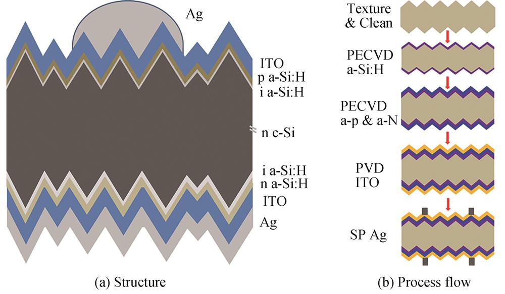
Fig. 1(a) shows the schematic structure of the SHJ devices, which is the sequence of Ag grid/ITO/(p)a-Si:H/(i)a-Si:H/(n)c-Si/(i)a-Si:H/(n)a-Si:H/ITO/Ag back contact. Fig. 1(b) shows the process flow of the SHJ solar cell. The full device processing sequence for SHJ solar cells comprises wet chemical treatments of the c-Si substrate and subsequent layer deposition. The n-type crystalline silicon (100) with a resistivity of 1~5 Ω·cm and thickness of 150 μm was acted as absorbing layer, ultra thin (i) a-Si:H film function as passivation layer, and (p)a-Si:H was employed as emitter layer, as well as forming p-n heterojunction with (n)c-Si, and (n)a-Si:H was as BSF. ITO target material (Sn:In2O3 resistivity≦0.14 mΩ·cm, purity 99.99%) was sputtered as transparent conductive oxide layer. Siver (Ag) was used as grid line and back contact.

Figure 1.Structure and process flow of SHJ solar cell
2.2 Wet-chemical treatment
Wet-chemical processes include removal of saw damage and a random pyramid surface texture etching. Sawing of the monocrystalline Si ingot into wafers contaminates the surfaces with the cutting slurry and creates crystal damages at the surfaces, as seen in Fig. 2(a). Thorough cleaning of the wafer and the complete removal of such saw damages are essential prerequisites for the reduction of recombination losses in Si solar cell. Fig. 2(b) shows an etching removal of at least 10 μm on each side to decrease effectively the surface roughness and to obtain the characteristic crystallographic features of the Si (100) surface[12].
Figure 2.SEM image of as-cut silicon wafer, wafer after saw damage etch, incompletely textured wafer, pyramid surface etched in 2% and 6% alkaline solutions and after chemical polishing
To improve the light trapping and thereby enhance the short-circuit current densities of the SHJ solar cell, particular emphasis is put on the wet-chemical random pyramid texturization of the solar cell substrates. Moreover, defects and contaminations on the surface can already be drastically reduced during the texturing process. Surface texturing is conventionally achieved by anisotropic wet-chemical etching of Si(100) wafers in alkaline solutions containing Isopropyl Alcohol (IPA) as an additive. Pyramid formation is due to the anisotropic reaction of alkali and silicon. In a certain concentration of alkaline solution, the reaction speed of OH- with the (100) surface of silicon is faster than that of the (111) surface. That is why the pyramid structure is formed[13]. Fig. 2(c) shows the etched surface of silicon wafer possibly due to low concentration KOH, short time etching or too much IPA additive. The typical process temperature is 70~80℃ below IPA boiling temperature, the nature of IPA is a stronger wetting function of the surface. This feature promotes a more homogeneous surface structure and allows to tune the pyramid size distribution. It is found the main factor that influence on the pyramid size is concentration of KOH in alkaline solutions. This behaviour can be explained by the morphological differences shown in the sequence of Scanning Electron Micrographs (SEM). Fig. 2(d) and (e) show the pyramid surface of wafers etched for 20 min in alkaline solutions with 2 wt% and 6 wt% KOH. The average pyramid sizes etched with 2 wt% KOH alkaline solution is around 2~4 μm, which increased to in the range of 6~9 μm etched with 6 wt% KOH alkaline solution. To smooth pyramid valleys and edges and increase crystallographic imperfections, the textured wafer was chemically polished with mixture solution of 95% HNO3 and 5% HF. Fig. 2(f) shows the morphological structure of textured surface after chemical polishing process. The distribution of the pyramids become more homogeneous, which is beneficial for wafer passivation by depositing intrinsic hydrogenated amorphous silicon film.
2.3 Interface passivation
Key feature of SHJ solar cell concept is a thin intrinsic amorphous hydrogenated silicon ((i) a-Si:H) layer which forms the heterocontact with a crystalline silicon (c-Si) wafer, provides passivation of the a-Si:H/c-Si interface, thus enables high open-circuit voltages (Voc). Further optimization of the a-Si:H/c-Si interface lead to an increase of the Voc, thereby an improvement of the solar cell performance[14]. A common technique to characterize the interface quality is to measure the carrier lifetime τeff as a function of the minority excess charge carrier density Δn by means of Transient Photoconductance Decay (TrPCD)[15].
Fig. 3(a) shows the reflectivity spectra of original, untreated textured wafers and textured wafers due to Chemical Polishing(CP). Obviously, the reflectivity of the textured c-Si wafer is around 10%, much lower than the raw wafer. Consequences of the texture-related improvement of the optical properties are both increase of the effective surface area and improved light trapping. After chemical polishing, the pyramid size distribution become more uniform, yielding lower reflection (Fig. 3(a)) than untreated textured wafer. After optimizing the texturization, the following process step is the cleaning of the wafer with RCA method. The Minority Carrier Lifetime (MCL) of textured wafer after cleaning was measured. As shown in Fig. 3(b), the MCL of as-cutting raw wafer is only 0.8 μs (inset of Fig. 3(b)), but the MCL of the textured wafer after cleaning and terminating with HF was more than 200 μs at an injection level of 1×1015 cm-3, which increased to 300 μs for the wafer underwent CP process. It is the fact that the wafer treated with CP was cleaner than the untreated wafer, because too small pyramids were eliminated and surfaces of the pyramids became smoothing after chemical polishing.
Figure 3.Reflectivity of original and textured wafers, MCL of passivated wafers affected by chemical polishing, pyramidsize and a-Si:H deposited at different temperatures
Optimization of texturization and cleaning was followed by intrinsic a-Si:H layers deposition, which are known to provide excellent passivation of the c-Si surfaces, causing a decrease of interface state density, mainly by hydrogenation of silicon dangling bonds. The a-Si:H thin film samples were prepared in a Radio Frequency (RF) 13.56 MHz and power density of 0.16 W/cm2 capacitive-coupled PECVD system. We deposited the textured wafer with the percentage content of silane SiH4 and dydrogen H2 at 220℃ under the chamber pressure of 1.5 (1 Torr=133.322 Pa). To get a high quality of a-Si:H passivated wafer, the window of deposition process is rather narrow. The influence of pyramid size on the effective minority charge carrier lifetime τeff after passivating with a-Si:H layer is summarized in Fig. 3(c). Samples with small size pyramids around 2~4 μm show lower carrier lifetimes of τeff < 2.5 ms, samples with pyramids around 6~9 μm reach higher values of up to 4.6 ms. For small pyramid wafer, the lifetime is limited by the increased influence of the valleys and edges which are known to be centres of epitaxial growth as well as starting points of local cracks in the (i) a-Si:H layer[16]. τeff rises with increasing fraction of bigger pyramids due to the lower density of pyramid free areas with (100) orientation, pyramid valleys and edges. It is indicated that 6~9 μm was suitable pyramid size for c-Si wafer passivation. Above a certain threshold, a further increase in pyramid size does not lead to a concomitant increase of the charge carrier lifetime and it is suggested that on textured surfaces with large pyramids the recombination processes at defects on the pyramid facets dominate the overall interface recombination[17].
The influence of the deposition temperature on τeff of textured c-Si wafers is shown in Fig. 3(d). It was found that increasing the temperature up to 220℃ leads to an increase of the charge carrier lifetime to a maximum value of 5.5 ms, which is promoted by the passivation of the (i)a-Si:H/c-Si interface by the highly mobile hydrogen. At 220℃ a trade-off between hydrogen concentration and mobility is reached, as has been confirmed by optical measurements that at lower substrate temperatures the (i)a-Si:H layer contains larger amounts of hydrogen[18]. However, at lower temperatures diffusion is limited and accordingly interface passivation is suppressed, which results in lower charge carrier lifetimes. Beyond 220℃ there is a decrease of τeff, possibly due to the lower hydrogen concentration or to increased interface recombination caused by local epitaxial growth, which is known as being detrimental for passivation[19]. Consequently, at Tsub=220℃ the largest carrier lifetimes are obtained owing to a high-quality (i)a-Si:H layer and a well passivated interface. At deposition temperatures >220℃ no improvement occurs due to partial deterioration of the a-Si:H interface[16].
2.4 Emitter and ITO optimization
In order to improve short wavelength photoresponse, p-type a-SiCx:H emitter was used in the SHJ solar cell absorption alternative to p-type a-Si:H[20]. Due to its broad band gap, the EQE of SHJ solar cell with p-type a-SiCx:H as emitter layer in short wavelength range of 300 to 600 nm is significantly higher than using p-type a-Si:H, as seen in Fig. 4(a).
Figure 4.Performances of SHJ solar cells
Eventually ITO layers were deposited on top Nip and back niN of the layer stack, respectively. ITO parasitic absorption in SHJ solar cell mainly includes the belt edge absorption and free carrier absorption. The former mainly affects the absorption of SHJ in the short wave region, while the latter affects the absorption in the long wave region. By 200℃ annealing after both the rear and front side ITO deposition, the ITO layer doping concentration was optimized to obtain a trade-off between low parasitic free-carrier absorption and low resistivity. The resistivity of 2.5×10⁻⁴ Ω·cm, highest carrier mobility of 31.8 cm2·V-1·s-1 and carrier concentration of 6.9×1020 cm-3 were obtained at Ar(O2) gas flow rate of 20 Sccm with the working pressure of 0.002 Torr. Using the optimized ITO layer with high charge carrier mobility and low resistivity in SHJ solar cell, the long wavelength response was obviously enhanced due to decrease of free carrier absorption, as shown in Fig. 4(b). In comparison to EQE data obtained for front- and rear-emitter silicon heterojunction solar cells on n- and p-type wafers presented recently by DESCOEUDRES A et al.[21], our cell suffers from losses in the long wavelength range (>1 000 nm) due to parasitic absorption in the doped ITO layer at the back side. By controlling the thickness of ITO at 100 nm, the reflectivity of the solar cell was further decreased, as shown in Fig. 4(c).
After metallic contacts were prepared and the characteristics of the solar cell were determined, the J-V curves of the 1 cm×1 cm cells were measured under standard test conditions with a shadow mask. The results of the best solar cell are given in Fig. 4(d), which shows a rather high efficiency above 21.68% after all the optimized processes. Thanks to excellent surface passivation, the Voc reaches 733 mV. The Jsc in J-V curve is well consistant with the Jsc integrated according to EQE (Fig. 4(c)). The fill factor is 76.8%, which is limited by thermal deposition of metallic contacts, the use of the silk-screen printing would be beneficial for further improvement of the solar cell.
4 Conclusion
Step-by-step optimization were analysed throughout the processing of SHJ solar cells starting from the pyramid structure etched Si wafer to the complete solar cell. Based on this investigation, recombination losses were successfully minimized and high open-circuit voltages and fill factors were obtained. Power conversion efficiencies above 21.68% were achieved by optimization of the texturing of silicon wafers, interface passivation, broad band gap emitter and ITO adjusting. The use of the silk-screen printing would be beneficial for further improvement of the solar cell.
References
[1] D JULIE, J QUENTIN, C JEAN et al. 23.5%-efficient silicon heterojunction silicon solar cell using molybdenum oxide as hole-selective contact. Nano Energy, 70, 104495(2020).
[2] A DESCOEUDRES, J HORZELl, B PAVIET‐SALOMON et al. The versatility of passivating carrier‐selective silicon thin films for diverse high‐efficiency screen‐printed heterojunction‐based solar cells. Progress in Photovoltaics: Research and Applications, 28, 569-577(2020).
[3] F GERENTON, J EYMARD, S HARRISON et al. Analysis of edge losses on silicon heterojunction half solar cells. Solar Energy Materials & Solar Cells, 204, 110213(2020).
[4] K YOSHIKAWA, H KAWASAKI, W YOSHIDA et al. Silicon heterojunction solar cell with interdigitated back contacts for a photoconversion efficiency over 26%. Nature Energy, 2, 817032(2017).
[5] M TAGUCHI, A YANO, S TOHODA et al. 24.7% record efficiency HIT solar cell on thin silicon wafer. IEEE Journal of Photovoltaics, 4, 96-99(2014).
[6] Zhenhai YANG, Xi YANG, Hao LIN et al. The role of transition region charges between dopant-free asymmetric heterocontacts in interdigitated back contact silicon heterojunction solar cells. Solar Energy, 188, 1201-1208(2019).
[7] Zhenhai YANG, Hao LIN, Jiang SHENG et al. Design principles of silicon heterojunction solar cells with dopant-free interdigitated back contacts. Solar RRL, 3, 1900230(2019).
[8] S D WOLF, M KONDO. Abruptness of a-Si:H/c-Si interface revealed by carrier lifetime measurements. Applied Physics Letters, 90, 042111(2007).
[9] L KORTE, E CONRAD, H R ANGERMANN et al. Advances in a-Si: H/c-Si heterojunction solar cell fabrication and characterization. Solar Energy Materials & Solar Cells, 93, 905-910(2009).
[10] S D WOLF, A DESCOEUDRES, Z HOLMAN et al. High-efficiency silicon heterojunction solar cells: a review. Green, 2, 7-24(2012).
[11] T KOIDA, H FUJIWARA, M KONDO. Reduction of optical loss in hydrogenated amorphous silicon/crystalline silicon heterojunction solar cells by high-mobility hydrogen-doped In2O3 transparent conductive oxide. Applied Physics Express, 1, 04501(2008).
[12] B STEGEMANNA, J KEGEL, M MEWS et al. Evolution of the charge carrier lifetime characteristics in crystalline silicon wafers during processing of heterojunction solar cells. Energy Procedia, 55, 219-228(2014).
[13] Y NISHIMOTO, K NAMBA. Investigation of texturization for crystalline silicon solar cells with sodium carbonate solutions. Solar Energy Materials & Solar Cells, 61, 393-402(2000).
[14] Yueke DING, Shihua HUANG. Study on passivation of monocrystalline silicon by tandem hydrogenated amorphous silicon film. Acta Photonica Sinica, 50, 0331001(2021).
[15] C LEENDERTZ, N MINGIRULLI, T SCHULZE et al. Discerning passivation mechanisms at a-Si:H/c-Si interfaces by means of photoconductance measurements. Applied Physics Letters, 98, 202108(2011).
[16] J KEGEL, H ANGERMKANN, U STURZEBECHER et al. IPA-free texturization of n-type Si wafers: correlation of optical, electronic and morphological surface properties. Energy Procedia, 38, 833-842(2013).
[17] S OLIBET, C MONACHON, A HESSLER-WYSER et al. Textured silicon heterojunction solar cells with over 700 mV open-circuit voltage studied by transmission electron microscopy, 1140(2008).
[18] B STEGEMANN, J KEGEL, M MEWS et al. Passivation of textured silicon wafers: influence of pyramid size distribution, a-Si:H deposition temperature, and post-treatment. Energy Procedia, 38, 881-889(2013).
[19] S D WOLF, H FUJIWARA, M KONDO. Impact of annealing on passivation of a-Si:H / c-Si heterostructures(2008).
[20] D ZHANG, D DELIGIANNIS, G PAPAKONSTANTINOU et al. Optical enhancement of silicon heterojunction solar cells with hydrogenated amorphous silicon carbide emitter. IEEE Journal of Photovoltaics, 4, 1326-1330(2014).
[21] A DESCOEUDRES, Z C HOLMAN, L BARRAUD et al. >21% efficient silicon heterojunction solar cells on n- and p-Type wafers compared. IEEE Journal of Photovoltaics, 3, 83-89(2013).