Directionally scattered surface plasmon polaritons (SPPs) promote the efficiency of plasmonic devices by limiting the energy within a given spatial domain, which is one of the key issues to plasmonic devices. Benefitting from the magnetic response induced in high-index dielectric nanoparticles, unidirectionally scattered SPPs have been achieved via interference between electric and magnetic resonances excited in the particles. Yet, as the magnetic response in low-index dielectric nanoparticles is too weak, the directionally scattered SPPs are hard to detect. In this work, we demonstrate forward scattered SPPs in single low-index polystyrene (PS) nanospheres. We numerically illustrate the excitation mechanism of plasmonic induced electric and magnetic multipole modes, as well as their contributions to forward SPP scattering of single PS nanospheres. We also simulate the SPP scattering field distribution obtaining a forward-to-backward scattering intensity ratio of 50.26:1 with 1 μm PS particle. Then the forward scattered SPPs are experimentally visualized by Fourier transforming the real-space plasmonic imaging to -space imaging. The forward scattered SPPs from low-index dielectric nanoparticles pave the way for SPP direction manipulation by all types of nanomaterials.
1. INTRODUCTION
Benefitting from the enhanced light–material interactions within nanoscales, plasmonic devices present a feasible resolution to the miniaturized and highly-integrated devices. Manipulating the directionality of surface plasmon polaritons (SPPs) limits the energy within a given spatial domain and thus promotes the efficiency of plasmonic devices. Traditionally, SPP directionality is achieved by breaking the symmetry of incidence and metallic structures or using specially arranged surface structures with SPP guiding properties. Normal incidence to asymmetric metallic structures induces the interference of SPPs to obtain unidirectionally propagated SPPs [1–3]. Also, oblique incidence interacting with symmetric structures generates asymmetric SPP excitation for directional SPP propagation [4–6]. SPP guiding is also achieved via chains, Y junction, triangle, and ring resonators of periodically arranged metallic nanoparticles based on localized surface plasmon scattering when the scatterers are located near a metal surface [7–9]. Yet, the above methods require precisely controlling the dimensions of metallic structures to satisfy the asymmetric SPP interference and excitation. Meanwhile, metallic structures induce high Ohmic losses and complex fabrication process, which hinders the development of plasmonic devices.
Recently, it was found that optically induced magnetic resonance can be excited in low loss high-index dielectric nanoparticles via circular displacement current induced by Mie scattering [10–13]. By the interference between electric and magnetic resonances excited in high-index dielectric nanoparticles, directional scattering is obtained [14,15]. Thereafter, people illustrated directional scattering in Si nanospheres [16,17], Si nanocubes [18], GaAs nanopillars [19], and Ge nanospheres [20]. By situating high-index dielectric nanoparticles on metallic film, directional SPP scattering is generated via constructive and destructive interference of electric and magnetic dipole moments in high-index dielectric nanoparticles. Evlyukhin and Bozhevolnyi investigated unidirectional SPP scattering of individual silicon (Si) nanoparticles on a gold film [21]. They numerically illustrated the electric and magnetic dipole resonances in Si nanoparticles, whose interaction induced the unidirectionally scattered SPPs. Sinev et al. demonstrated the directivity switching of scattered SPPs via controlling the effective elliptical electric polarization of a single Si nanoparticle, which is induced by the phase delay between the electric and magnetic dipole responses [22]. Kang et al. investigated directional SPP excitation via interference between SPPs with phase difference launched by a pair of Si cuboids with different sizes [23].
Compared with high-index dielectric nanoparticles, their low-index dielectric counterparts, i.e., and polystyrene (PS) nanoparticles, have low costs, stable performance, and wide applications. Yet, the low index of particles is considered to weaken the coupling between incident light and electromagnetic eigenmodes, leading to weak Mie resonances. People have investigated the optically induced electric and magnetic responses in low-index dielectric particles. In 2018, Zhou et al. enhanced the magnetic dipole moments with partial metal dressing and visualized the directional scattering of single nanoparticles [24]. Then, Abdelrahman et al. demonstrated zero backward scattering at the microwave band by exciting high-order electric and magnetic multipole modes in PMMA particles [25,26]. Furthermore, Zhang et al. found highly forward scattering of PS nanoparticles induced by interference between electric and magnetic multipole modes utilizing highly efficient coloring solar cells [27]. These investigations give a ray of hope to directionally scattered SPPs by using single low-index dielectric nanoparticles. Although it has been proven that an optically induced magnetic response exists in low-index dielectric nanoparticles and generates directional scattering via interference with electric response, the mechanism of plasmonic induced magnetic response in low-index dielectric nanoparticles is still in absence. Also, no demonstration for directional SPP scattering of low-index dielectric nanoparticles has been implemented.
Sign up for Photonics Research TOC. Get the latest issue of Photonics Research delivered right to you!Sign up now
In this work, we present the directionally (forward) scattered SPPs by situating PS nanospheres on Au film. We indicate the contributions of electric and magnetic multipole modes to the forward SPP scattering in single PS nanospheres. The forward-to-backward ratio of scattering intensity increases with particle size, theoretically 50.26:1 with particle diameter being 1 μm. We also experimentally demonstrate forward SPP scattering via Fourier transforming the real-space plasmonic imaging of single PS nanospheres to -space imaging. The directionally scattered SPPs of low-index dielectric nanospheres open new practical ways to plasmonic devices and extend the SPP manipulation to all kinds of dielectric materials.
2. THEORETICAL APPROACH AND SIMULATIONS
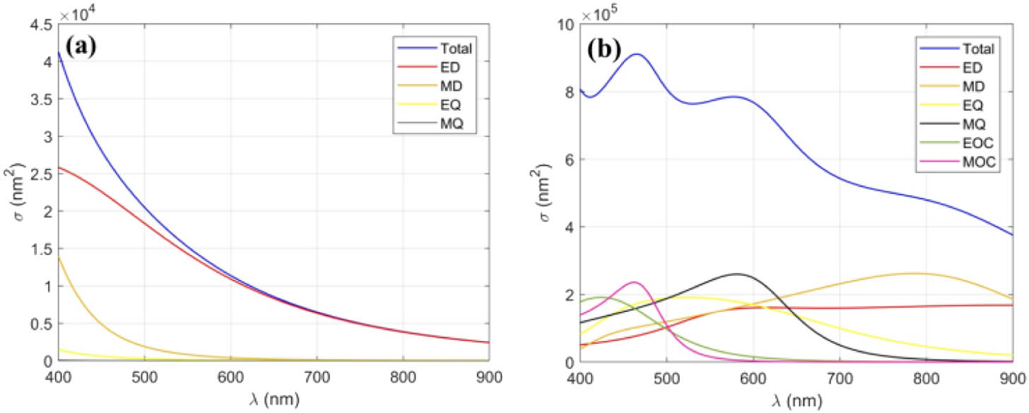
We propose a model by situating a single PS nanosphere on Au film. The launched SPP wave propagating along the Au–air interface interacts with the PS nanosphere. We employ multipole expansion analysis by using a combination of numerical calculation of the electric field and decomposition discrete dipole approximation (DDDA) to clarify the contributions of electric and magnetic responses to SPP directional scattering (see Appendix A and Ref. [28]). First, using Mie theory [29], we consider the free-space scattering cross sections (SCSs) and their corresponding multipole decompositions of a PS sphere with diameter being 200 nm [Fig. 1(a)] and of a PS sphere with diameter being 500 nm [Fig. 1(b)]. In the former case, the SCS is determined by contributions of only first low-order multipole moments such as the electric dipole (ED), magnetic dipole (MD), electric quadrupole (EQ), and magnetic quadrupole (MQ). In the latter case of a bigger particle, the SCS includes contributions of the magnetic quadrupole (MQ), electric octupole (EOC), and magnetic octupole (MOC). Thus, with particle size increasing, more electric and magnetic multipole modes participate in the scattering, providing realization of the Mie scattering regime with dominate scattering in the forward direction [30].
Figure 1.Free-space scattering cross sections of PS nanospheres (the refractive index is 1.6) with diameter being (a) 200 nm and (b) 500 nm. ED, electric dipole; MD, magnetic dipole; EQ, electric quadrupole; MQ, magnetic quadrupole; EOC, electric octupole; MOC, magnetic octupole.
Similar to free-space scattering, SPP scattering is also determined by the contributions of electric and magnetic multipole modes excited in the scatterer by external waves. Figures 2(a) and 2(b) demonstrate the electric and magnetic multipole decomposition of SPP scattering by the PS nanospheres with diameters being 200 and 500 nm, respectively. For a small PS nanoparticle with 200 nm diameter, the ED, MD, and EQ modes contribute to the weak forward scattering [Fig. 2(a)]. With diameter increasing to 500 nm, besides the ED, MD, and EQ modes, the MQ and EOC modes are also excited, providing strong forward SPP scattering with suppression of the backward scattering. Such behavior corresponds to the transition from the symmetric Rayleigh scattering regime to the asymmetric Mie scattering regime with the increase of the scatterer size as it takes place for light scattering in free space by dielectric spheres.
Figure 2.In-plane angle distribution of the SPP scattering intensity (TOTAL) by the PS nanospheres with diameter being (a) 200 nm and (b) 500 nm. Combination of the multipole contributions: ED, electric dipole; MD, magnetic dipole; EQ, electric quadrupole; MQ, magnetic quadrupole; EOC, electric octupole; MOC, magnetic octupole. The forward scattering corresponds to ; for the backward scattering . The incident SPP’s frequency corresponds to the light with the wavelength of 600 nm in free space.
In order to illustrate the excitation mechanism of electric and magnetic multipole modes in the PS nanosphere, we simulate the electric and magnetic field amplitude distribution by using commercial FDTD software from Lumerical Solutions, Inc. [31] (the details of the simulation refer to Appendix B). Figure 3(a) shows the simulated electric field amplitude distribution at plane with displacement vector distributions of single PS nanospheres interacting with SPPs, with sphere diameters being 200 nm, 500 nm, and 1 μm. With nanosphere diameters being 200 nm, the electric field concentrates within the gap between nanosphere and interface. Also, a weak current loop appears around the gap, which indicates the weak magnetic dipole mode excited by the mirror effect of the nanosphere on the metallic film, as the simulated magnetic field amplitude distribution of 200 nm PS nanospheres shown in Fig. 3(b). In Fig. 3(c), we also simulate the surface charge distribution to illustrate the electric dipole moment in the 200 nm PS nanosphere. With the diameter increasing to 500 nm, the current loop in the PS nanosphere splits to two parts [Fig. 3(a)], indicating the magnetic quadrupole mode excited in the particle [Fig. 3(b)]. Figure 3(c) manifests that the electric quadrupole mode is excited in the nanosphere and induces the magnetic quadrupole mode located in the 500 nm PS nanosphere. Furthermore, with the particle sizing up to 1 μm, higher-order electric and magnetic modes emerge in the PS particle showing stronger magnetic modes. As a result, with particle size increasing, higher-order electric and magnetic modes are induced in the PS particle.
Figure 3.SPP interacting with PS spheres of different diameters of 200 nm, 500 nm, and 1000 nm. SPP propagates along axis with the wavevector as shown in (a). (a) Simulated electric field amplitude distribution with displacement vector, (b) simulated magnetic field amplitude distribution , and (c) simulated surface charge distribution, simulated electric field component amplitude distribution. The incident SPP’s frequency corresponds to the light with the wavelength of 600 nm in free space.
Due to the evanescent characteristics of SPPs, we also simulate the amplitude distribution of electric and magnetic field components , , and at plane with particle diameter being 200 nm, 500 nm, and 1 μm, respectively, as shown in Appendix C. For particle diameter being 200 nm, is weak, and both and concentrate within the gap between nanosphere and interface. With diameter increasing to 500 nm, is still weak but manifests quadrupole modes in the particle. Besides being located within the particle–interface gap, both electric and magnetic quadrupole modes of and , i.e., modes, emerge in the particle. When particle size increases to 1 μm, higher-order TM mode with stronger amplitudes appear in the particle. Furthermore, the interference between electric and magnetic modes leads to enhanced scattering intensity in the forward direction and suppresses the scattering in the backward direction. For small PS particles, the weak electric and magnetic modes induced by and result in weak forward SPP scattering. With the particle sizing up to 500 nm, strong electric and magnetic quadrupole modes of and emerge in the particle, and the directionality of forward SPP scattering increases. When the PS particle size increases to 1 μm, the higher-order multipole modes of are excited in the particle, and , , and all contribute to forward SPP scattering.
We calculate the electric field intensity distribution of scattered SPPs (Appendix D), as shown in Figs. 4(a)–4(e). With the SPP wavelength being 600 nm, the scattered intensity concentrates along the SPP propagation direction, and forward SPP scattering is illustrated. Moreover, with particle size increasing from 200 nm to 1 μm, the directionality starts to be more pronounced. Additionally, the spatial frequency spectra of scattered SPPs are obtained by Fourier transforming the near-field electric field to -space (Appendix D), as shown in Figs. 4(f)–4(j). In order to quantify the directionality of the scattered SPPs, we transform the rectangular coordinates to polar coordinates to obtain the angular radiation distribution. In Figs. 4(k)–4(o), with the particle sizing up, the lobes of SPP scattering narrow down, indicating that the scattering field concentrates in the forward direction. The forward-to-backward scattering intensity ratio is 2.49, 11.13, 28.99, 37.78, and 50.26, respectively, which displays the increasing ratio with sizing up (Appendix E).
Figure 4.Electric field intensity distribution of scattered SPPs with particle diameters being (a) 200 nm, (b) 300 nm, (c) 500 nm, (d) 800 nm, and (e) 1 μm. The spatial frequency spectra of SPP scattering in -space with particle diameters being (f) 200 nm, (g) 300 nm, (h) 500 nm, (i) 800 nm, and (j) 1 μm. The angular distribution of SPP scattering of single PS particle with diameters being (k) 200 nm, (l) 300 nm, (m) 500 nm, (n) 800 nm, and (o) 1 μm. The forward-to-backward scattering intensity ratios are 2.49, 11.13, 28.99, 37.78, and 50.26, respectively.
We measure the forward SPP scattering experimentally by using plasmonic imaging to single PS nanospheres. Figure 5 shows the schematic of the experimental setup to observe forward SPP scattering. A 633 nm He–Ne laser (JDSU 1135P) is employed to excite SPPs by using the objective-coupled Kretschmann configuration. A polarizer is inserted into the optical path to deliver the p-polarized light for SPP excitation. An oil immersion objective (Olympus APON100×HOTIRF) with is used for both SPP excitation and light collection. By adjusting the linear stage (LS) to control the incident angle, the SPPs are excited at the Au–air interface. We deposit PS nanospheres on 50 nm thickness Au film evaporated on a cover glass substrate. The nanospheres disperse sufficiently to facilitate the imaging for single nanospheres (Appendix F). The single PS nanospheres interact with SPPs and generate SPP scattering delivered to the far field [32]. After passing through a beam-splitter prism, partial scattering signals are captured by the CCD1 camera (AVT Guppy Pro F146B) for real-space imaging. The rest passes through Lens3 for Fourier transformation, and is captured by the CCD2 camera (Alvium 1800 U-507m) for -space imaging.
Figure 5.Experimental setup of measurement to forward scattered SPPs.
The PS nanospheres with diameters of 200 nm, 300 nm, 500 nm, 800 nm, and 1 μm are used to measure the directionality of scattered SPPs. In the measurement, the interference between SPPs and reflection background is collected by the CCD1 camera. Data processing is required to eliminate the reflection background. We averaged 20 images to reduce the experimental errors and subtracted the reflection background without nanospheres as well as the dark noise of CCD1. Figures 6(f)–6(j) show the real-space imaging to a single PS nanosphere characterized by bright spots with parabolic fringes, which is consistent with the simulated near field electric field intensity , as shown in Figs. 6(a)–6(e) (Appendix G). In Figs. 6(k)–6(o), we also obtain the spatial frequency spectra of scattered SPP intensity in -space via CCD2 by image averaging and dark noise subtraction. The bright spot in the circle along the incident direction represents the launched SPPs, and the circle manifests the scattered SPPs in -space with nonuniform intensity angular distribution, which demonstrates the scattered SPPs occurring more efficiently in the forward direction.
Figure 6.Simulated SPP electric field intensity distribution at in real space of single PS nanospheres with diameters being (a) 200 nm, (b) 300 nm, (c) 500 nm, (d) 800 nm, and (e) 1 μm. manifests the propagating direction of SPPs. Experimental real-space imaging to single PS nanospheres with diameters of (f) 200 nm, (g) 300 nm, (h) 500 nm, (i) 800 nm, and (j) 1 μm. Experimental -space imaging to single PS nanospheres with diameters being (k) 200 nm, (l) 300 nm, (m) 500 nm, (n) 800 nm, and (o) 1 μm.
Due to the interference between scattered SPPs and launched SPPs , it is hard to obtain the scattered SPPs from -space imaging experimentally. We retrieve the intensity of scattered SPPs approximately by subtracting the -space imaging without nanoparticles from that with nanoparticles, i.e., . Twenty -space images with and without nanoparticles as and are obtained and retrieve the intensity of scattered SPPs in -space. Figures 7(a)–7(e) show the scattered SPP distribution of single PS nanospheres in -space imaging with particle diameters of 200 nm, 300 nm, 500 nm, 800 nm, and 1 μm. After transforming the rectangular coordinates to polar coordinates, the angular radiation distributions are shown in Figs. 7(f)–7(j). With the particle diameter being 200 nm, 300 nm, 500 nm, 800 nm, and 1 μm, the forward-to-backward scattering intensity ratio is 10.27, 19.98, 35.83, 25.55, and 22.44, respectively. The maximum forward-to-backward ratio appears at 500 nm diameter. We do not observe the obviously narrow trend of the scattering lobe, because the scattered SPPs of single 200 nm and 300 nm PS particles are too weak to observe. With particle diameter increasing from 500 nm to 1 μm, the lobes of the approximately scattered SPPs show a tendency to narrow down. We also measure the scattered SPPs of single 300 nm Au nanospheres (Appendix H). A uniform intensity angular distribution in -space imaging indicates nondirectional SPP scattering. As only localized surface plasmons are excited in metal particles, no directional SPP scattering emerges with the absence of magnetic response. By comparison with nondirectional SPP scattering of gold particles, the induced magnetic response in low-index dielectric particles and forward scattered SPPs is confirmed.
Figure 7.Experimental results of SPP scattering intensity of single PS nanospheres with diameters of (a) 200 nm, (b) 300 nm, (c) 500 nm, (d) 800 nm, and (e) 1 μm in -space. The corresponding angular radiation distribution of PS nanospheres with diameters being (f) 200 nm, (g) 300 nm, (h) 500 nm, (i) 800 nm, and (j) 1 μm; the forward-to-backward scattering intensity ratios are 10.27, 19.98, 35.83, 25.55, and 22.44, respectively. Approximately simulated results of scattered SPPs with particle diameters being (k) 200 nm, (l) 300 nm, (m) 500 nm, (n) 800 nm, and (o) 1 μm. Corresponding angular radiation distribution of particles with diameters being (p) 200 nm, (q) 300 nm, (r) 500 nm, (s) 800 nm, and (t) 1 μm; the forward-to-backward scattering intensity ratios are 6.59, 20.43, 38.53, 28.22, and 25.3, respectively.
As the experimental results are retrieved approximately by subtracting the -space imaging without nanoparticles from that with nanoparticles, we employ the same processing method in approximately simulated results (Appendix D). Figures 7(k)–7(o) show the approximately simulated SPP scattering intensity with particle diameters of 200 nm, 300 nm, 500 nm, 800 nm, and 1 μm. In Figs. 7(p)–7(t), we obtain their angular radiation distribution. The angular radiation distribution shows the forward-to-backward scattering intensity ratio being 6.59, 20.43, 38.53, 28.22, and 25.3, respectively, with the particle sizing up. The maximum ratio appears at 500 nm diameter, which is consistent with the experimental results.
We compare the forward-to-backward scattering intensity ratio between experiment and simulation, and the discrepancy is shown in Fig. 10 (Appendix I). The size parameter “” () is used to indicate the relationship between particle diameter and wavelength, in which is the particle diameter and is the SPP wavelength. With the SPP wavelength being 600 nm, the size parameters “” are 1.05, 1.57, 2.62, 4.19, and 5.23 with particle diameter being 200 nm, 300 nm, 500 nm, 800 nm, and 1 μm. The experimental results are consistent with approximately simulated results with maximum forward-to-backward ratio at 500 nm particle diameter. Meanwhile, the experimental results indicate discrepancy with simulations.
4. CONCLUSIONS
In summary, we investigate the SPP-induced magnetic multipole modes and theoretically and experimentally demonstrate the forward SPP scattering in single low-index PS nanospheres. Numerically, we indicate the excitation mechanism of electric and magnetic multipole modes in single PS particles. The forward SPP scattering is induced by interference between electric and magnetic multipole modes including the high order modes such as octupole and higher ones. Contributions of these modes into the scattering lead to the realization of a Mie scattering regime with predominant forward scattering. We demonstrate numerically that the forward-to-backward scattering intensity ratio increases to 50.26:1 with the particle sizing up to 1 μm. In experimental demonstration, by tuning the diameter of PS nanospheres, the maximum forward-to-backward scattering intensity ratio being 35.83:1 is visualized with particle diameter being 500 nm. The directionally scattered SPPs in low-index dielectric nanoparticles pave the way for the optical field manipulation to more materials that break through the limitations of nanophotonics and extend its application to photonics chips integration and meta-devices widely.
Acknowledgment
Acknowledgment. We thank Prof. Weili Zhang from Tianjin University, Prof. Shaopeng Wang from Arizona State University, Dr. Jing Zhou from Shanghai Institute of Technical Physics, Chinese Academy of Sciences, Dr. Muyuan Yang from Qsinghua University, and Dr. Wei Xiong from Institute of Microelectronics, Chinese Academy of Sciences, for their useful discussion. The DDDA multipole analysis was supported by the Deutsche Forschungsgemeinschaft (DFG, German Research Foundation) under Germany’s Excellence Strategy within the Cluster of Excellence PhoenixD.
APPENDIX A: DDDA FOR SPP MULTIPOLE SCATTERING
For multipole analysis of SPP scattering by dielectric spheres we applied the method combining the numerical calculation of the electric field in the scatterer and the DDDA [28]. Here we briefly indicate the main stages of our approach. Using the Lumerical calculation facilities, we simulate the SPP scattering by the dielectric sphere and obtain the electric fields inside all discrete cells belonging to the scatterer ( is the number of a cell). The electric dipole moments of all cells are determined as , , where is the vacuum dielectric constant, and are the dielectric permittivities of the scatterer and the medium above metal substrate, respectively, and is the volume of the corresponding discretization cell. Then the discrete representation of the induced polarization inside the scatterer is , where is the total number of the dipoles inside the scatterer, is the Dirac delta function, and is the radius-vector of the th cell. Using the dicrete representation of , the multipole moments of the scatterer are calculated from the expressions presented in Ref. [33]. For example, the ED (), MD (), and EQ () and MQ () moments can be written as where is the wave number in the medium with , is the angular frequency of SPP waves, and is the spherical Bessel function of the th order, . The multipole moments are located at the center of the spherical scatterer.
The multipole decomposition of the electric field of SPP scattered waves is written as [28] where is the wave number in vacuum, is the angular frequency of the SPP, is the radius-vector of the scatterer’s center of mass, is the SPP wave vector, the vector , , is the in-plane angle determining the direction of the observation point with , and is the permittivity of the metal substrate. The tensor depends on only the coordinate of the observation point. Expressions for the electric fields of SPP waves radiated by high multipole moments can be obtained from the corresponding expressions for the electric and magnetic dipoles by applying the general rule described in Ref. [28]. The electric and magnetic fields of the SPP waves generated by the electric and magnetic dipoles are shown in Ref. [28]. For calculation of SPP scattering directivity, we need only the out-of-plane component of the electric field of the scattered SPP wave.
The SPP power scattered by the scatterer located near a metal surface into an in-plane angle is determined by the expression where the component (out-of-plane) of the scattered SPP electric field is taken on the metal surface from the side of the scatterer. Note that the above expression was obtained by neglecting the imaginary part of substrate metal permittivity . Using the electric field as a superposition of multipole contributions, the importance of different multipoles in the scattered SPP power can be estimated. Figure 2 presents the function calculated for different number of multipole moments.
APPENDIX B: FDTD SIMULATION
All of the simulation results in this manuscript are executed by the commercial FDTD software from Lumerical Solutions, Inc. The total field scattered field (TFSF) plane wave is used as the simulation source. The incident wavelength for SPP excitation is 633 nm, and the SPP wavelength is around 600 nm. The simulation mesh is , and the Au–air interface is set as plane . The light source is positioned at , with size being 6 μm in both the and directions. The emission direction is along the axis, and the polarization direction is along the axis. The single nanoparticle is positioned at the center with coordinate (0, 0, ) with refractive index being 1.6. The simulation domain is 6 μm in both the and axes containing three media with air (), Au (), and glass (). The perfectly matched layer (PML) is set as the boundary condition. The simulation time is set to be 1000 fs, and the simulation auto shutoff is , which ensures a sufficiently long simulation time for valid simulated results.
APPENDIX C: THE SIMULATION OF ELECTRIC AND MAGNETIC FIELD COMPONENTS
We simulate the amplitude distribution of electric and magnetic field components , , and at plane with particle diameter being 200 nm, 500 nm, and 1 μm, respectively, as shown in Fig. 8.
Figure 8.Simulated electric field component amplitude distribution (a) , (b) , and (c) simulated magnetic field component amplitude distribution of single PS nanospheres at plane . Incident SPP’s frequency corresponds to the light with the wavelength of 600 nm in free space.
Electric Field Intensity Distribution of Scattered SPPs
We simulate the complex electric field with single nanoparticles , in which represents the launched SPPs and represents the scattered SPPs. Also, the simulated complex electric field of launched SPPs without single nanoparticles is simulated. The electric field intensity distribution of scattered SPPs is calculated as .
Spatial Frequency Spectra of Scattered SPPs
The spatial frequency spectra of scattered SPPs are calculated as . We calculate the complex electric field of scattered SPPs by subtracting from . Then, the complex electric field of scattered SPPs in -space is retrieved by Fourier transformation. The spatial frequency spectra of scattered SPPs are obtained via squaring the absolute value of scattered SPPs in -space.
Approximately Simulated Scattered SPPs
In the experiment, we obtain the real-space imaging of single nanoparticles with the interference between launched SPPs and scattered SPPs , . The experimental result of scattered SPP intensity is approximately as . In order to approximate the experimental results, we employ the same processing method in approximately simulated results by subtracting the -space imaging without nanoparticles from that with nanoparticles, i.e., .
APPENDIX E: CALCULATION OF FORWARD-TO-BACKWARD RATIO OF DIRECTIONALLY SCATTERED SPPs
For calculating the forward-to-backward scattering intensity ratio, the spatial frequency spectra of scattered SPPs of a single PS nanoparticle in -space under rectangular coordinates (, ) transform to polar coordinates (, ). We use software Image J to transform the rectangular coordinates to polar coordinates and calculate the angular distribution of the scattered SPP intensity. We obtain the forward SPP scattering intensity by adding the scattering intensity up from to , and the backward SPP scattering by adding the scattering intensity up from to . Finally, we obtain the forward-to-backward intensity ratio of directionally scattered SPPs.
APPENDIX F: SAMPLE PREPARATION
The PS nanoparticles with diameter being 200 nm, 500 nm, and 1 μm were purchased from Alfa Aesar (China) Chemical Co., Ltd. The PS nanoparticles with 300 nm and 800 nm diameters were purchased from Beijing Biotyscience Technology Co., Ltd. In order to prevent the nanoparticles from clustering, the nanoparticle solution is diluted with anhydrous alcohol to around . First, the cover glass coated with Au film is positioned on the hotplate, and the diluted nanoparticle solution is dripped on the Au film with the dropping pipette. The hotplate is used to accelerate the evaporation, which makes the nanoparticles adsorbed on Au film dispersively before they cluster. The nanoparticle sample is monodispersed until the anhydrous alcohol is evaporated.
APPENDIX G: SIMULATION OF REAL-SPACE IMAGING TO SINGLE PS NANOSPHERES
As the far-field real-space imaging to single nanospheres is the projection of the near-field electric field intensity distribution at the Au–air interface via the leakage radiation [34], we simulate the near-field electric field intensity to reflect the real-space imaging. The real-space imaging to single PS nanospheres is calculated as , in which . We simulate the near-field electric field intensity at plane with nanoparticles as and electric field intensity of launched SPPs without nanoparticles , respectively. Then we subtract the electric field intensity without particles from those with nanoparticles . The simulated SPP electric field distribution at near-field plane in real space is obtained.
APPENDIX H: MEASUREMENT OF SCATTERED SPPs OF SINGLE AU NANOSPHERES
We measure the SPP scattering of single 300 nm Au nanospheres by using plasmonic imaging. Figure 9(a) shows the real-space imaging of single Au nanospheres. Figure 9(b) indicates the measured -space imaging subtracting reflection background, i.e., launched SPPs. An almost uniform circle indicates the weak directionality of SPP scattering induced by single Au nanospheres. Transforming the -space imaging to angular radiation distribution [in Fig. 9(c)], the forward-to-backward scattering intensity ratio is calculated to be 4.53.
Figure 9.(a) Real-space imaging of single 300 nm Au nanospheres. (b) -space imaging subtracting launched SPPs. (c) Angular radiation distribution of scattered SPPs of single 300 nm Au nanospheres.
APPENDIX I: COMPARISON OF FORWARD-TO-BACKWARD SCATTERING INTENSITY RATIOS BETWEEN EXPERIMENT, SIMULATION, AND APPROXIMATELY SIMULATED RESULTS
In Fig. 10(a), we compare the experiment, simulation, and approximately simulated results. The size parameter () is used to indicate the relationship between particle diameter and wavelength, in which is the particle diameter and is the SPP wavelength. With SPP wavelength being 600 nm, the size parameters are 1.05, 1.57, 2.62, 4.19, and 5.23 with particle diameter being 200 nm, 300 nm, 500 nm, 800 nm, and 1 μm, respectively. The experimental results are consistent with approximately simulated results with maximum forward-to-backward ratio at (500 nm particle diameter). Meanwhile, the experimental results indicate a discrepancy with the simulations. In order to figure out the discrepancy, we calculate the forward and backward scattering intensity in Fig. 10(b). For , the approximately simulated results manifest higher increasing speed of forward scattering intensity and lower decreasing speed of backward scattering intensity, leading to larger forward-to-backward scattering intensity ratios compared with simulations. For , the backward scattering intensity of the approximately simulated result indicates lower decreasing speed in Fig. 10(c), leading to smaller forward-to-backward scattering intensity ratios compared with simulations.
Figure 10.(a) Comparison of the forward-to-backward scattering intensity ratios among experiment, simulation, and approximately simulated results. (b) Comparison of the forward and backward scattering intensity of PS nanospheres between simulation and approximately simulated results. (c) Enlargement of the backward scattering of PS nanoparticle with diameter being 500 nm, 800 nm, and 1 μm in (b).