• Photonics Research
  • Vol. 10, Issue 11, 2575 (2022)
Wei Ke1, Yanmei Lin1, Mingbo He1, Mengyue Xu1, Jiaxiang Zhang2, Zhongjin Lin3、4、*, Siyuan Yu1, and Xinlun Cai1、5、*
Author Affiliations
  • 1State Key Laboratory of Optoelectronic Materials and Technologies, School of Electronics and Information Technology, Sun Yat-sen University, Guangzhou 510275, China
  • 2State Key Laboratory of Functional Materials for Informatics, Shanghai Institute of Microsystem and Information Technology, Chinese Academy of Sciences, Shanghai 200092, China
  • 3Department of Electrical and Computer Engineering, The University of British Columbia, Vancouver, British Columbia V6T 1Z4, Canada
  • 4e-mail:
  • 5e-mail:
  • show less
    DOI: 10.1364/PRJ.471534 Cite this Article Set citation alerts
    Wei Ke, Yanmei Lin, Mingbo He, Mengyue Xu, Jiaxiang Zhang, Zhongjin Lin, Siyuan Yu, Xinlun Cai. Digitally tunable optical delay line based on thin-film lithium niobate featuring high switching speed and low optical loss[J]. Photonics Research, 2022, 10(11): 2575 Copy Citation Text show less
    (a) Schematic of the proposed 4-bit tunable optical delay line. PD, photodetector. (b) Architecture of 2 × 2 Mach–Zehnder interferometer (MZI) switch and its cross section. (c) Transmission spectrum of MZI switch with the applied voltage. (d) Transmission spectrum of MZI switch at bar/cross states. (e) Fast-switching spectrum of MZI when applied a 1 MHz square wave.
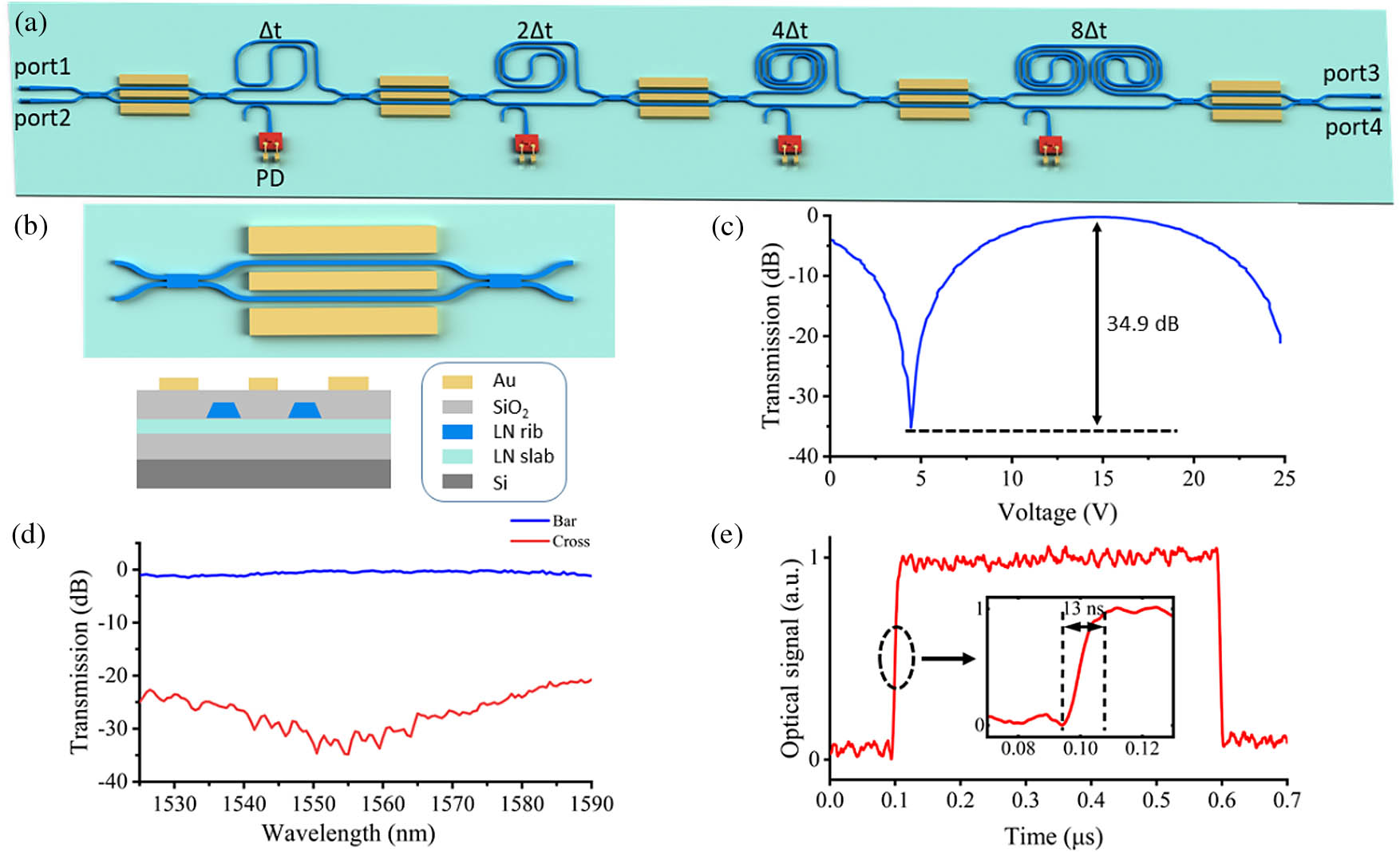
    Fig. 1. (a) Schematic of the proposed 4-bit tunable optical delay line. PD, photodetector. (b) Architecture of 2 × 2 Mach–Zehnder interferometer (MZI) switch and its cross section. (c) Transmission spectrum of MZI switch with the applied voltage. (d) Transmission spectrum of MZI switch at bar/cross states. (e) Fast-switching spectrum of MZI when applied a 1 MHz square wave.
    Comparison of arc bend and modified Euler bend. The schematics and corresponding simulation results of (a) modified Euler-bend waveguide and (b) regular arc bend waveguide with the same radius of 46 μm and width of 2.2 μm, respectively.
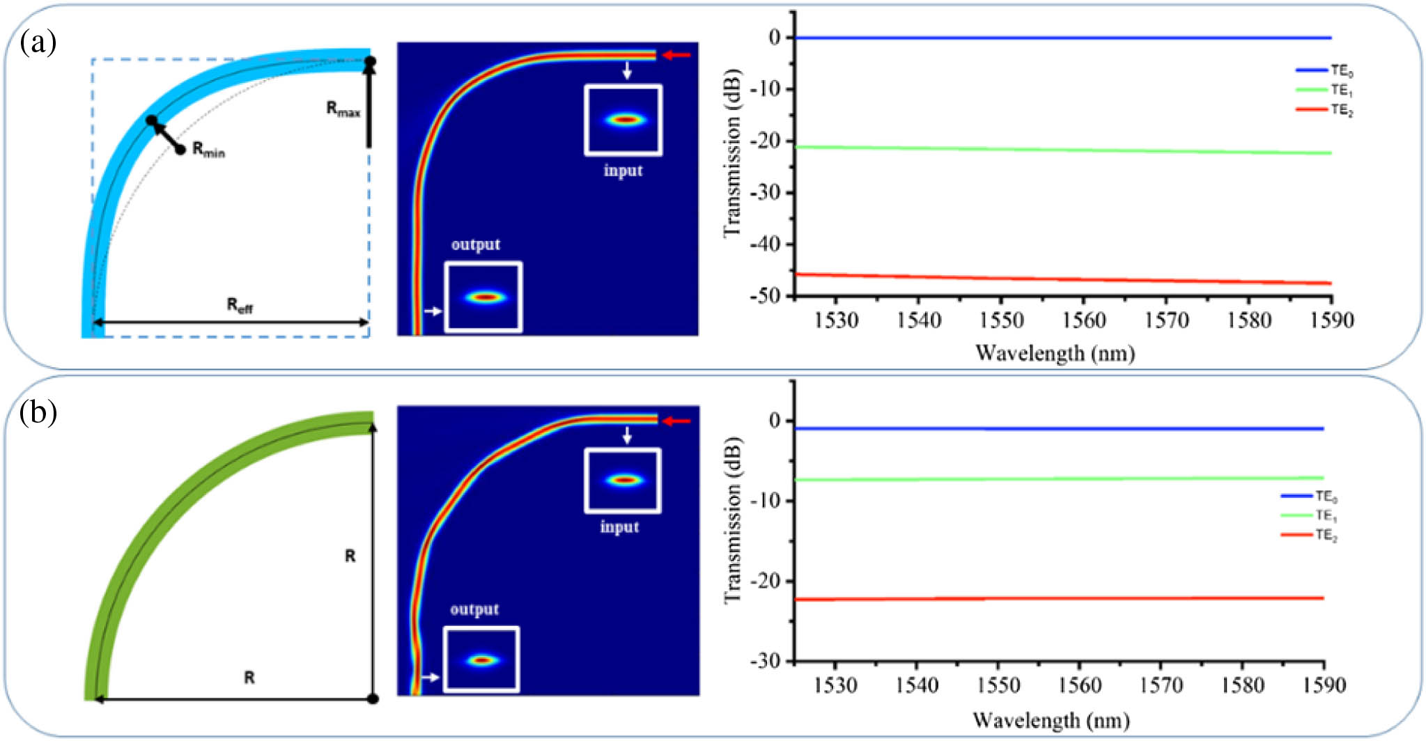
    Fig. 2. Comparison of arc bend and modified Euler bend. The schematics and corresponding simulation results of (a) modified Euler-bend waveguide and (b) regular arc bend waveguide with the same radius of 46 μm and width of 2.2 μm, respectively.
    (a) Microscopy image of the fabricated device and one of the MZI switches. Microscopy of (b) back-sensing on-chip photodiode and (c) delay-line waveguide spiral with a delay of 80 ps used in the proposed device, respectively.
    Fig. 3. (a) Microscopy image of the fabricated device and one of the MZI switches. Microscopy of (b) back-sensing on-chip photodiode and (c) delay-line waveguide spiral with a delay of 80 ps used in the proposed device, respectively.
    (a) Experimental setup for optical delay characterization. PC, polarization controller; MZM, Mach–Zehnder modulator; ADC/DAC, analog-to-digital converter/digital-to-analog converter; TIA, trans-impedance amplifier; ODL, optical delay line; PD, photodetector; VNA, vertical network analyzer. (b) Schematic of the optical path for different delay times. (c) Comparison between theoretical and measured delay times. (d) Optical insertion loss for different delay times.
    Fig. 4. (a) Experimental setup for optical delay characterization. PC, polarization controller; MZM, Mach–Zehnder modulator; ADC/DAC, analog-to-digital converter/digital-to-analog converter; TIA, trans-impedance amplifier; ODL, optical delay line; PD, photodetector; VNA, vertical network analyzer. (b) Schematic of the optical path for different delay times. (c) Comparison between theoretical and measured delay times. (d) Optical insertion loss for different delay times.
    (a) and (b) show the schematics of the optical paths and the corresponding transmission optical power when the delay time is tuned between 150 and 100 ps and between 150 and 20 ps, respectively.
    Fig. 5. (a) and (b) show the schematics of the optical paths and the corresponding transmission optical power when the delay time is tuned between 150 and 100 ps and between 150 and 20 ps, respectively.
    Fabrication flow of the proposed optical delay line. HSQ, hydrogen silsesquioxane; PMMA, polymethylmethacrylate.
    Fig. 6. Fabrication flow of the proposed optical delay line. HSQ, hydrogen silsesquioxane; PMMA, polymethylmethacrylate.
    (a) Simulated effective index of the waveguide in the y direction and z direction varying with wavelength. (b) Measured delay time of the fabricated waveguide spirals with different lengths.
    Fig. 7. (a) Simulated effective index of the waveguide in the y direction and z direction varying with wavelength. (b) Measured delay time of the fabricated waveguide spirals with different lengths.
    Two square waves applied to the switches and corresponding transmission optical power.
    Fig. 8. Two square waves applied to the switches and corresponding transmission optical power.
    (a) Schematic of a 1-bit tunable optical delay line (ODL). (b) Switching time of ODL varying with the switching time of the single switch. (c), (d) Simulation results when switching time of switch is set at 10 ns and 50 ps, respectively.
    Fig. 9. (a) Schematic of a 1-bit tunable optical delay line (ODL). (b) Switching time of ODL varying with the switching time of the single switch. (c), (d) Simulation results when switching time of switch is set at 10 ns and 50 ps, respectively.
     MaterialDelay Range (ps)Resolution (ps)Delay Loss (dB/ps)Power Efficiency (mW/ps)Switching Timea (μs)Footprint (mm2)
    7-bit ODL [7]SOI191.371.420.11.2633.722.23
    7-bit ODLb [14]SOI1270100.0090.0518.9728.62
    4-bit ODL [18]Si3N4/SiO212,3508500.0010.02-3825
    4-bit ODL [21]Polymer17711.80.0840.82800297
    4-bit ODL [35]Silica90.260.0261.47840602
    Our workTFLN150100.023Negligiblec0.01350
    Table 1. Comparison of Various Switchable Delay Lines
    Wei Ke, Yanmei Lin, Mingbo He, Mengyue Xu, Jiaxiang Zhang, Zhongjin Lin, Siyuan Yu, Xinlun Cai. Digitally tunable optical delay line based on thin-film lithium niobate featuring high switching speed and low optical loss[J]. Photonics Research, 2022, 10(11): 2575
    Download Citation