
Wei Ke, Yanmei Lin, Mingbo He, Mengyue Xu, Jiaxiang Zhang, Zhongjin Lin, Siyuan Yu, Xinlun Cai. Digitally tunable optical delay line based on thin-film lithium niobate featuring high switching speed and low optical loss[J]. Photonics Research, 2022, 10(11): 2575
- Photonics Research
- Vol. 10, Issue 11, 2575 (2022)
Abstract
1. INTRODUCTION
Optical delay lines (ODLs) have been applied in various fields, such as optical communication, microwave photonics, and optical coherence tomography [1–3]. For example, in optical signal processing, ODLs are used for feed-forward optical buffers and time-slot interchange units in future low-power-consumption and low-latency optical switching systems [4–6]. In microwave photonic systems, ODLs can be used as a key building block of microwave photonic beamformers in future compact size and large bandwidth radar systems [7–9]. To date, most commercial ODLs are still based on fiber-optic or free-space optical components [10–13] and generally require moving parts to achieve tunable operation; these parts are bulky in size, slow in response time, and cumbersome to use. Therefore, a tunable, compact, and low-cost ODL is highly desirable for integrated waveguide platforms.
In recent decades, several tunable ODLs based on different waveguide platforms have been proposed and experimentally demonstrated, such as silicon (Si), silicon nitride (), silica, and polymers [14–21]. Most of the demonstrated tunable ODLs rely on the thermo-optic effect, resulting in a low switching speed and high power consumption. Using the plasma dispersion effect, a tunable ODL based on a silicon-on-insulator or indium phosphide can achieve nanosecond-level tuning speed. However, such a device suffers from high optical insertion loss and limited extinction ratio owing to free carrier absorption [22,23].
Recently, thin-film lithium niobate (TFLN) has emerged as an attractive material platform for high-performance photonic integrated devices [24]. For example, TFLN-based optical modulators with electro-optic (EO) bandwidths greater than 100 GHz and half-wave voltages of 1 V have been demonstrated [25–27]. TFLN-based polarization management devices have recently been demonstrated to simultaneously feature low optical loss, high-speed operation, compact size, and low drive voltage [28]. With the advantages of high-speed operation and low optical loss, TFLN is also an ideal material platform for realizing a high-performance tunable ODL. A TFLN-based tunable ODL has been reported previously with ultra-low loss delay waveguides; however, the fast electrical tuning operation of the ODL has not yet been demonstrated [29].
Sign up for Photonics Research TOC. Get the latest issue of Photonics Research delivered right to you!Sign up now
In this study, we propose a digitally 4-bit tunable ODL based on the TFLN platform comprising cascaded Mach–Zehnder interferometer (MZI) optical switches, flip-chip bonded monitoring photodetectors (MPDs), and four delay-line waveguide spirals. This device can achieve a maximum delay time of 150 ps with a resolution of 10 ps. The insertion loss for the 150 ps delay time is 3.4 dB, corresponding to a delay loss of 0.023 dB/ps. The present device exhibits a switching speed of 13 ns between two arbitrary delays, which is the best value in the integrated tunable ODLs.
2. CONCEPT AND BUILDING BLOCKS
As shown in Fig. 1(a), the proposed device consists of five MZI optical switches, four delay-line waveguide spirals, four reference line waveguides, and four flip-chip bonded MPDs. The delay times of the four delay waveguides were 10, 20, 40, and 80 ps. The present device can provide a tunable delay time from 0 to 150 ps with a resolution of 10 ps by controlling the cross/bar states of the optical switches. Each reference line waveguide has a 1:99 directional coupler and a grating coupler. The outputs of the grating coupler are coupled to the flip-chip bonded MPDs, which are used to provide feedback on the cross/bar states of the optical switches. The device was designed and fabricated using an X-cut lithium niobate on insulator (LNOI) platform with a device layer thickness of 360 nm and buried oxide layer thickness of 4.7 μm. The waveguide was ridge-type with a height of 180 nm and a slab thickness of 180 nm. In the following, we discuss the details of the proposed optical switches and delay-line waveguide spirals.
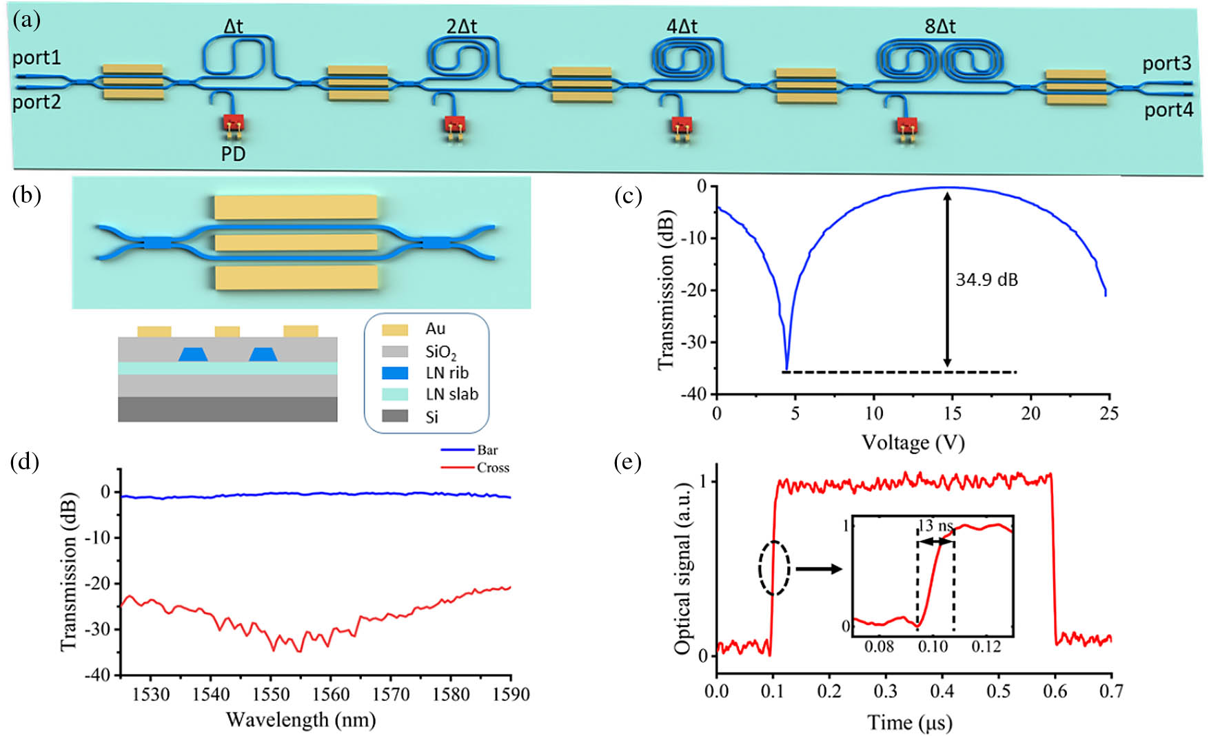
Figure 1.(a) Schematic of the proposed 4-bit tunable optical delay line. PD, photodetector. (b) Architecture of 2 × 2 Mach–Zehnder interferometer (MZI) switch and its cross section. (c) Transmission spectrum of MZI switch with the applied voltage. (d) Transmission spectrum of MZI switch at bar/cross states. (e) Fast-switching spectrum of MZI when applied a 1 MHz square wave.
TFLN-based optical switches are critical elements of the ODL device, as shown in Fig. 1(b). The optical splitters/combiners of the MZI were implemented using 3 dB multimode interferometer (MMI) couplers. The MZI operates in a single-drive push–pull configuration such that the electric fields induce phase shifts with an equal magnitude but opposite signs in the two arms. The arm length of the MZI was 2.5 mm. The gap between the electrodes and the width of the optical waveguide in between are 3.4 μm and 2 μm, respectively. The half-wave voltage of the device was measured as 10 V, corresponding to a length-voltage product of . The extinction ratio of the MZI optical switch is measured to be as high as 34.9 dB, owing to the large fabrication tolerance of the MMI coupler. Moreover, the device exhibited an extinction ratio larger than 25 dB in the wavelength range of 1530–1575 nm [Fig. 1(d)]. High speed is one of the most prominent advantages of the TFLN-based optical switches. As shown in Fig. 1(e), the device can achieve a switching time of 13 ns, which is limited by the rising edge of the driving signal (1 MHz square wave). The proposed device does not experience the direct current (DC) bias draft [28,30].
A delay-line waveguide spiral is an important component. The spiral delay-line waveguide is composed of several bend and straight waveguides [Fig. 1(a)]. A modified Euler-bend multimode waveguide design was employed to reduce propagation loss [31–34]. The modified Euler-bend curve is defined as follows:
Figure 2 shows a comparison of the regular arc bend and modified Euler-bend waveguides. Both the regular arc bend and modified Euler-bend waveguides were simulated with the same footprint of and a width of 2.2 μm. Figure 2(a) indicates that when injecting a fundamental transverse electric field () with a wavelength of 1550 nm, the mode propagates smoothly in the 90° modified Euler-bend waveguide, and no notable inter-mode is observed. Moreover, the corresponding transmission spectrum shows that the high-order modes excited in the modified Euler-bend waveguide are lower than . In contrast, a significant multimode inference occurred in the regular arc-bend waveguide [Fig. 2(b)].
![]()
Figure 2.Comparison of arc bend and modified Euler bend. The schematics and corresponding simulation results of (a) modified Euler-bend waveguide and (b) regular arc bend waveguide with the same radius of 46 μm and width of 2.2 μm, respectively.
Based on the wide waveguides and modified Euler bend, the delay-line waveguide spirals can simultaneously achieve low loss and compactness. The distance between two adjacent waveguides was set to 10 μm, sufficient to avoid evanescent coupling. In this case, waveguide spirals with lengths greater than 1.57 cm can be placed in an area of . Since the widths of waveguides in the optical switches and delay-line waveguide spirals are different, they are connected with MMI couplers through different tapers.
3. FABRICATION AND EXPERIMENTS
The fabrication process is detailed in the Appendix A. Figure 3(a) presents a microscopy image of the fabricated tunable ODL, and the inset of Fig. 3(a) presents a magnified image of one MZI switch. The footprint of the fabricated device is . Figures 3(b) and 3(c) present the microscopy images of the flip-chip MPDs and modified Euler-bend-based waveguide spiral, respectively. As discussed in Appendix B, the average group index of the waveguide spiral is 2.245. Therefore, the total length of the delay-line waveguide of the proposed device is 2 cm.
![]()
Figure 3.(a) Microscopy image of the fabricated device and one of the MZI switches. Microscopy of (b) back-sensing on-chip photodiode and (c) delay-line waveguide spiral with a delay of 80 ps used in the proposed device, respectively.
A. Characterization of Delay Time
A schematic of the experimental setup used for measuring the delay time of the ODL is shown in Fig. 4(a). The delay time can be obtained by comparing the output microwave signal generated by the vector network analyzer (VNA) and its local replica. In the experiment, the wavelength of the tunable laser was set as 1550 nm. More details about the experiment, including the calibration of the voltage applied to each optical switch, can be found in Appendix C.
![]()
Figure 4.(a) Experimental setup for optical delay characterization. PC, polarization controller; MZM, Mach–Zehnder modulator; ADC/DAC, analog-to-digital converter/digital-to-analog converter; TIA, trans-impedance amplifier; ODL, optical delay line; PD, photodetector; VNA, vertical network analyzer. (b) Schematic of the optical path for different delay times. (c) Comparison between theoretical and measured delay times. (d) Optical insertion loss for different delay times.
We applied combinations of voltages to the tunable ODL to generate six different delay times, ranging from 0 to 150 ps [Fig. 4(b)]. Figure 4(c) shows the measured delay times, consistent with the expected values. The optical losses of the fabricated device for different delay times are shown in Fig. 4(d). The maximum and minimum on-chip insertion losses of the tunable ODL were 3.4 dB and 2.5 dB, respectively. The on-chip loss for 3.4 dB can be broken down as follows: the losses for the delay-line waveguides and five optical switches are 0.9 dB and 2.5 dB, respectively. The insertion loss of the proposed device can be further decreased after improving the fabricated processing.
B. High-Speed Tunability Experiment
To demonstrate the performance of high-speed tunability, the delay time of our device was switched between 100 and 150 ps and between 20 and 150 ps, respectively [Figs. 5(a) and 5(b)]. Four square-wave electrical signals with a repetition rate of 125 kHz and a sampling rate of 2 MHz, generated from the multifunction I/O module (NI PXIe-6363), were simultaneously applied to the four optical switches, while a constant electrical signal was applied to the remaining optical switch. The output optical powers are presented at the bottom of Figs. 5(a) and 5(b), indicating that the switching time of the fabricated ODL can achieve 0.5 μs. The switching speed of the proposed ODL is limited by the speed of the electrical control system. Using a higher-speed electrical control system, the switching time of the fabricated ODL can be further improved to be close to 13 ns. (Details can be found in Appendix D.) In theory, the switching time of the proposed tunable ODL is equal to the sum of maximum delay time and switching time of the single optical switch as discussed in Appendix E.
![]()
Figure 5.(a) and (b) show the schematics of the optical paths and the corresponding transmission optical power when the delay time is tuned between 150 and 100 ps and between 150 and 20 ps, respectively.
4. CONCLUSIONS
Based on the TFLN platform, a tunable ODL with a maximum delay time of 150 ps and a resolution of 10 ps was proposed and experimentally demonstrated. The proposed optical switch exhibits a switching speed of 13 ns and an extinction ratio of 34.9 dB, which outperforms other tunable ODLs as shown in Table 1. Moreover, using the modified Euler bends to build the delay-line waveguide, the maximum optical insertion loss of the proposed tunable ODL is only 3.4 dB. With its advantages of low optical loss and fast switching speed, the proposed device has significant potential in optical communication, microwave photonics, optical autocorrelators, and optical coherence tomography applications. Comparison of Various Switchable Delay Lines The switching time of other ODLs is the switching time of a single switch. Only switchable delay line is in consideration. Our device only consumes power when driving voltages are changing. Delay Range Resolution Delay Loss Power Efficiency Switching Footprint 7-bit ODL [ SOI 191.37 1.42 0.1 1.26 33.7 22.23 7-bit ODL SOI 1270 10 0.009 0.05 18.97 28.62 4-bit ODL [ 12,350 850 0.001 0.02 - 3825 4-bit ODL [ Polymer 177 11.8 0.084 0.8 2800 297 4-bit ODL [ Silica 90.2 6 0.026 1.47 840 602 Our work TFLN 150 10 0.023 Negligible 0.013 50
Acknowledgment
Acknowledgment. We thank Lidan Zhou, Lin Liu, and Shengqian Gao for their technical support.
APPENDIX A: FABRICATION OF THE PROPOSED DEVICE
The fabrication process of the proposed device is shown in Fig.
![]()
Figure 6.Fabrication flow of the proposed optical delay line. HSQ, hydrogen silsesquioxane; PMMA, polymethylmethacrylate.
APPENDIX B: GROUP INDEX OF WAVEGUIDE SPIRAL
The effective index of the waveguide in the direction and direction varying with the wavelength is shown in Fig.
![]()
Figure 7.(a) Simulated effective index of the waveguide in the
APPENDIX C: DETAILS OF THE CHARACTERIZATION OF DELAY
The measurement setup is shown in Fig.
First, we calibrated the bias voltage of the device. In principle, the initial state of a single switch should be at the cross state. However, the bias voltage required for each switch to reach the initial state needs to be calibrated due to fabrication imperfection. The PXI multifunction I/O module can not only be used as a multichannel voltage source to drive the optical switches of device, but also read the output voltages of the flip-chip bonded MPD. We wrote a program on LabVIEW to display the real-time input and output voltage of the PXI multifunction I/O module. According to the optical power feedback from the flip-chip MPD, we confirmed the switching voltage of switches one by one as shown in Table Switching Voltages of Switches (in V) Switch1 Switch2 Switch3 Switch4 Switch5 Bar 4.8 –6.7 5.4 –8 –7 Cross –5.9 3.1 –4.2 2.6 2.9
APPENDIX D: HIGH-SPEED TUNABILITY EXPERIMENT
With the limitation of our experiment setup, we cannot simultaneously generate four square waves with high repetition rate and high amplitude. Therefore, to show the shortest switching time of our device, we used a two-channel arbitrary waveform generator to control two switches, while the other three remained bar state constant. As shown in Fig.
![]()
Figure 8.Two square waves applied to the switches and corresponding transmission optical power.
APPENDIX E: THEORETICAL SHORTEST SWITCHING TIME OF THE PROPOSED ODL
In theory, the switching time of the proposed tunable ODL is equal to the sum of the maximum delay time and the switching time of the single optical switch. To demonstrate this, as shown in Fig.
![]()
Figure 9.(a) Schematic of a 1-bit tunable optical delay line (ODL). (b) Switching time of ODL varying with the switching time of the single switch. (c), (d) Simulation results when switching time of switch is set at 10 ns and 50 ps, respectively.
References
[1] D. Gauthier. Slow light brings faster communications. Phys. World, 18, 30-32(2005).
[2] J. T. Mok, B. J. Eggleton. Photonics: expect more delays. Nature, 433, 811-812(2005).
[13] M. Yessenov, A. F. Abouraddy. Demonstration of a free-space optical delay line using space-time wave packets. Frontiers in Optics + Laser Science APS/DLS, FW1C.1(2019).
[17] Z. Ke, R. Ge, X. Cai. Tunable optical true time delay line based on ring array. Asia Communications and Photonics Conference (ACP), S3F.4(2018).
[19] K. Horikawa, I. Ogawa, H. Ogawa, T. Kitoh. Photonic switched true time delay beam forming network integrated on silica waveguide circuits. Proceedings of 1995 IEEE MTT-S International Microwave Symposium, 61, 65-68(1995).
[20] M. S. Rasras, J. L. Grange, C. K. Madsen, M. A. Cappuzzo, E. Chen, L. Gomez, E. J. Laskowski, A. Griffin, A. Wong-Foy, A. Kasper, S. S. Patel. Integrated scalable continuously tunable variable optical delay lines. IEEE LEOS Annual Meeting Conference Proceedings, 736-737(2005).

Set citation alerts for the article
Please enter your email address
© Copyright 2018-2021 | Chinese Laser Press. All Rights Reserved 沪ICP备15018463号-20