
Haiyang Li, Qiaoxia Li, Zhaoba Wang, Qianghua Pan. Detection and Evaluation of Surface Defects Based on Critical Frequency Method by Laser Ultrasonic[J]. Acta Optica Sinica, 2018, 38(7): 0712003
- Acta Optica Sinica
- Vol. 38, Issue 7, 0712003 (2018)
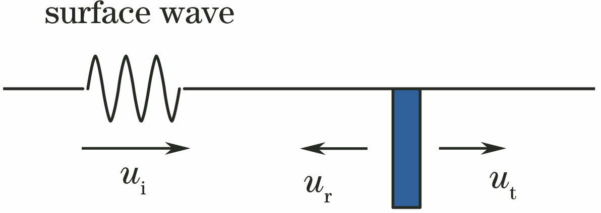
Fig. 1. Scattering effect between surface wave and defect
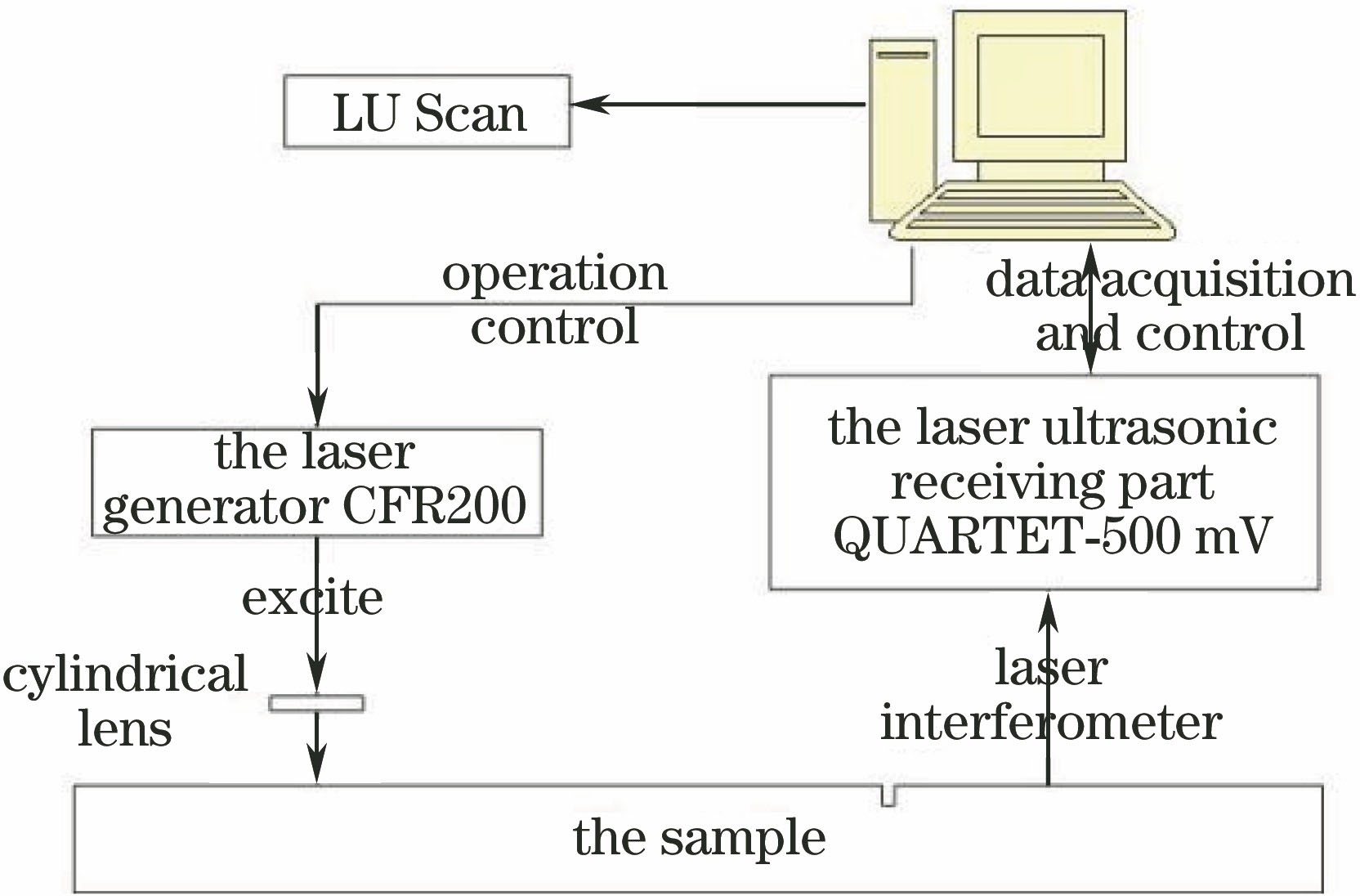
Fig. 2. Experimental diagram
Fig. 3. Laser ultrasonic platform
Fig. 4. Experimental samples
Fig. 5. Sample size
Fig. 6. Direct wave spectrum diagram
Fig. 7. B-scanning images of surface defect. (a) Defect depth of 0.40 mm; (b) defect depth of 0.30 mm; (c) defect depth of 0.20 mm; (d) defect depth of 0.10 mm; (e) defect depth of 0.08 mm
Fig. 8. Frequency spectrum energy diagrams of reflection/transmission signals. (a) Defect depth of 0.40 mm; (b) defect depth of 0.30 mm; (c) defect depth of 0.20 mm; (d) defect depth of 0.10 mm; (e) defect depth of 0.08 mm (red solid lines and blue solid lines represent curves of transmission surface wave and defect reflection surface wave, respectively)
Fig. 9. Relationship between surface defect depth and corresponding wavelength
Fig. 10. B-scanning images at different distances between excitation point and detection point
Fig. 11. Frequency spectrum energy diagrams of reflection/transmission signal when distance between excitation point and detection point is different. (a) Distance of 5 mm; (b) distance of 10 mm ; (c) distance of 15 mm; (d) distance of 20 mm; (e) distance is of 25 mm (the red solid lines and blue solid lines represent curves of transmission surface wave and defect reflection surface wave, respectively)
Fig. 12. Samples with different materials. (a) Steel sample; (b) aluminum sample
Fig. 13. Frequency spectrum energy diagrams of reflection/transmission signals of samples with different materials. (a) Aluminum; (b) steel (the red solid lines and blue solid lines represent curves of transmission surface wave and defect reflection surface wave, respectively)
|
Table 1. Defect depth
|
Table 2. Measured location and error of defects
|
Table 3. Measured defect depth and error
|
Table 4. Measured defect depth and error at different distances between excitation point and detection point
|
Table 5. Defect depth and error of samples with different materials

Set citation alerts for the article
Please enter your email address
© Copyright 2018-2021 | Chinese Laser Press. All Rights Reserved 沪ICP备15018463号-20